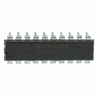
MCHC908JK3ECPE Freescale Semiconductor, MCHC908JK3ECPE Datasheet - Page 95
MCHC908JK3ECPE
Manufacturer Part Number
MCHC908JK3ECPE
Description
IC MCU 4K FLASH 8MHZ 20-DIP
Manufacturer
Freescale Semiconductor
Series
HC08r
Datasheet
1.MC908JK1ECDWE.pdf
(180 pages)
Specifications of MCHC908JK3ECPE
Core Processor
HC08
Core Size
8-Bit
Speed
8MHz
Peripherals
LED, LVD, POR, PWM
Number Of I /o
15
Program Memory Size
4KB (4K x 8)
Program Memory Type
FLASH
Ram Size
128 x 8
Voltage - Supply (vcc/vdd)
2.7 V ~ 3.3 V
Data Converters
A/D 12x8b
Oscillator Type
External
Operating Temperature
-40°C ~ 85°C
Package / Case
20-DIP (0.300", 7.62mm)
Processor Series
HC08JK
Core
HC08
Data Bus Width
8 bit
Data Ram Size
128 B
Maximum Clock Frequency
8 MHz
Number Of Programmable I/os
23
Number Of Timers
2
Operating Supply Voltage
2.7 V to 5.5 V
Maximum Operating Temperature
+ 85 C
Mounting Style
Through Hole
Development Tools By Supplier
FSICEBASE, DEMO908JL16E, M68CBL05CE
Minimum Operating Temperature
- 40 C
On-chip Adc
8 bit, 12 Channel
Lead Free Status / RoHS Status
Lead free / RoHS Compliant
Eeprom Size
-
Connectivity
-
Lead Free Status / Rohs Status
Details
Available stocks
Company
Part Number
Manufacturer
Quantity
Price

Part Number:
MCHC908JK3ECPE
Manufacturer:
FREESCALE
Quantity:
20 000


8.9.5 TIM Channel Registers (TCH0H/L:TCH1H/L)
These read/write registers contain the captured TIM counter value of the input capture function or the
output compare value of the output compare function. The state of the TIM channel registers after reset
is unknown.
In input capture mode (MSxB:MSxA = 0:0), reading the high byte of the TIM channel x registers (TCHxH)
inhibits input captures until the low byte (TCHxL) is read.
In output compare mode (MSxB:MSxA ≠ 0:0), writing to the high byte of the TIM channel x registers
(TCHxH) inhibits output compares until the low byte (TCHxL) is written.
Freescale Semiconductor
Address:
Address:
Address:
Address:
Reset:
Reset:
Reset:
Reset:
Read:
Read:
Read:
Read:
Write:
Write:
Write:
Write:
Figure 8-9. TIM Channel Registers (TCH0H/L:TCH1H/L)
$0026
$0027
$0029
Bit15
Bit15
$02A
Bit 7
Bit 7
Bit 7
Bit 7
Bit7
Bit7
TCH0H
TCH1H
TCH0L
TCH1L
Bit14
Bit14
Bit6
Bit6
MC68HC908JL3E Family Data Sheet, Rev. 4
6
6
6
6
Bit13
Bit13
Bit5
Bit5
5
5
5
5
Indeterminate after reset
Indeterminate after reset
Indeterminate after reset
Indeterminate after reset
Bit12
Bit12
Bit4
Bit4
4
4
4
4
Bit11
Bit11
Bit3
Bit3
3
3
3
3
Bit10
Bit10
Bit2
Bit2
2
2
2
2
Bit9
Bit1
Bit9
Bit1
1
1
1
1
Bit 0
Bit 0
Bit 0
Bit 0
Bit8
Bit0
Bit8
Bit0
I/O Registers
95
Related parts for MCHC908JK3ECPE
Image
Part Number
Description
Manufacturer
Datasheet
Request
R

Part Number:
Description:
Manufacturer:
Freescale Semiconductor, Inc
Datasheet:
Part Number:
Description:
Manufacturer:
Freescale Semiconductor, Inc
Datasheet:
Part Number:
Description:
Manufacturer:
Freescale Semiconductor, Inc
Datasheet:
Part Number:
Description:
Manufacturer:
Freescale Semiconductor, Inc
Datasheet:
Part Number:
Description:
Manufacturer:
Freescale Semiconductor, Inc
Datasheet:
Part Number:
Description:
Manufacturer:
Freescale Semiconductor, Inc
Datasheet:
Part Number:
Description:
Manufacturer:
Freescale Semiconductor, Inc
Datasheet:
Part Number:
Description:
Manufacturer:
Freescale Semiconductor, Inc
Datasheet:
Part Number:
Description:
Manufacturer:
Freescale Semiconductor, Inc
Datasheet:
Part Number:
Description:
Manufacturer:
Freescale Semiconductor, Inc
Datasheet:
Part Number:
Description:
Manufacturer:
Freescale Semiconductor, Inc
Datasheet:
Part Number:
Description:
Manufacturer:
Freescale Semiconductor, Inc
Datasheet:
Part Number:
Description:
Manufacturer:
Freescale Semiconductor, Inc
Datasheet:
Part Number:
Description:
Manufacturer:
Freescale Semiconductor, Inc
Datasheet:
Part Number:
Description:
Manufacturer:
Freescale Semiconductor, Inc
Datasheet: