MCF52100CAE80 Freescale Semiconductor, MCF52100CAE80 Datasheet - Page 33
MCF52100CAE80
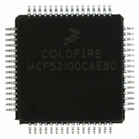
Manufacturer Part Number
MCF52100CAE80
Description
IC MCU 32BIT 80MHZ 64-LQFP
Manufacturer
Freescale Semiconductor
Series
MCF521xxr
Datasheet
1.MCF52110CAF80.pdf
(56 pages)
Specifications of MCF52100CAE80
Core Processor
Coldfire V2
Core Size
32-Bit
Speed
80MHz
Connectivity
I²C, SPI, UART/USART
Peripherals
DMA, LVD, POR, PWM, WDT
Number Of I /o
43
Program Memory Size
64KB (64K x 8)
Program Memory Type
FLASH
Ram Size
16K x 8
Voltage - Supply (vcc/vdd)
3 V ~ 3.6 V
Data Converters
A/D 8x12b
Oscillator Type
Internal
Operating Temperature
-40°C ~ 85°C
Package / Case
64-LQFP
Processor Series
MCF521x
Core
ColdFire V2
Data Bus Width
32 bit
Data Ram Size
16 KB
Interface Type
I2C/QSPI/UART
Maximum Clock Frequency
80 MHz
Number Of Programmable I/os
56
Number Of Timers
10
Operating Supply Voltage
- 0.3 V to + 4 V
Maximum Operating Temperature
+ 85 C
Mounting Style
SMD/SMT
3rd Party Development Tools
JLINK-CF-BDM26, EWCF
Development Tools By Supplier
M52210DEMO
Minimum Operating Temperature
- 40 C
On-chip Adc
8-ch x 12-bit
For Use With
M5211DEMO - KIT DEMO FOR MCF5211
Lead Free Status / RoHS Status
Lead free / RoHS Compliant
Eeprom Size
-
Lead Free Status / Rohs Status
Lead free / RoHS Compliant


Electrical Characteristics
1
2
3
4
5
6
7
8
9
10
11
2.9
GPIO can be configured for certain pins of the QSPI, DDR Control, timer, UART, and Interrupt interfaces. When in GPIO mode,
the timing specification for these pins is given in
The GPIO timing is met under the following load test conditions:
33
Frequency un-LOCK range
Frequency LOCK range
CLKOUT period jitter
On-chip oscillator frequency
• Peak-to-peak (clock edge to clock edge)
• Long term (averaged over 2 ms interval)
In external clock mode, it is possible to run the chip directly from an external clock source without enabling the PLL.
This value has been updated.
All internal registers retain data at 0 Hz.
Depending on packaging; see the orderable part number summary.
Loss of Reference Frequency is the reference frequency detected internally, which transitions the PLL into self clocked mode.
Self clocked mode frequency is the frequency at which the PLL operates when the reference frequency falls below f
default MFD/RFD settings.
This parameter is characterized before qualification rather than 100% tested.
Proper PC board layout procedures must be followed to achieve specifications.
This specification applies to the period required for the PLL to relock after changing the MFD frequency control bits in the
synthesizer control register (SYNCR).
Jitter is the average deviation from the programmed frequency measured over the specified interval at maximum f
Measurements are made with the device powered by filtered supplies and clocked by a stable external clock signal. Noise
injected into the PLL circuitry via V
for a given interval.
Based on slow system clock of 40 MHz measured at f
NUM
G1
G2
G3
G4
•
•
50 pF / 50 for high drive
25 pF / 25 for low drive
General Purpose I/O Timing
4, 5, 10 ,11
CLKOUT High to GPIO Output Invalid
CLKOUT High to GPIO Output Valid
CLKOUT High to GPIO Input Invalid
Table 28. Oscillator and PLL Electrical Specifications (continued)
GPIO Input Valid to CLKOUT High
Characteristic
, measured at f
Characteristic
DDPLL
(V
DD
MCF52110 ColdFire Microcontroller, Rev. 1
and V
and V
SYS
SSPLL
DDPLL
Table 29
Table 29. GPIO Timing
Max
and variation in crystal oscillator frequency increase the C
= 2.7 to 3.6 V, V
sys
and
max.
Figure
5.
SS
Symbol
C
f
f
= V
f
LCK
oco
UL
jitter
Symbol
t
t
CHPOV
t
CHPOI
t
SSPLL
PVCH
CHPI
= 0 V)
–0.75
–1.5
7.84
Min
—
—
Min
1.5
1.5
—
9
Freescale Semiconductor
Max
0.75
8.16
1.5
.01
10
Max
10
—
—
—
jitter
percentage
sys
% f
LOR
% f
% f
MHz
Unit
.
Unit
sys
ns
ns
ns
ns
ref
ref
with
Related parts for MCF52100CAE80
Image
Part Number
Description
Manufacturer
Datasheet
Request
R

Part Number:
Description:
Manufacturer:
Freescale Semiconductor, Inc
Datasheet:
Part Number:
Description:
Manufacturer:
Freescale Semiconductor, Inc
Datasheet:
Part Number:
Description:
Manufacturer:
Freescale Semiconductor, Inc
Datasheet:
Part Number:
Description:
Manufacturer:
Freescale Semiconductor, Inc
Datasheet:
Part Number:
Description:
Manufacturer:
Freescale Semiconductor, Inc
Datasheet:
Part Number:
Description:
Manufacturer:
Freescale Semiconductor, Inc
Datasheet:
Part Number:
Description:
Manufacturer:
Freescale Semiconductor, Inc
Datasheet:
Part Number:
Description:
Manufacturer:
Freescale Semiconductor, Inc
Datasheet:
Part Number:
Description:
Manufacturer:
Freescale Semiconductor, Inc
Datasheet:
Part Number:
Description:
Manufacturer:
Freescale Semiconductor, Inc
Datasheet:
Part Number:
Description:
Manufacturer:
Freescale Semiconductor, Inc
Datasheet:
Part Number:
Description:
Manufacturer:
Freescale Semiconductor, Inc
Datasheet:
Part Number:
Description:
Manufacturer:
Freescale Semiconductor, Inc
Datasheet:
Part Number:
Description:
Manufacturer:
Freescale Semiconductor, Inc
Datasheet:
Part Number:
Description:
Manufacturer:
Freescale Semiconductor, Inc
Datasheet: