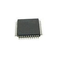
MC9S08JM16CLD Freescale Semiconductor, MC9S08JM16CLD Datasheet - Page 252

MC9S08JM16CLD
Manufacturer Part Number
MC9S08JM16CLD
Description
MCU 8BIT 16K FLASH 44-LQFP
Manufacturer
Freescale Semiconductor
Series
HCS08r
Datasheet
1.DEMO9S08JM16.pdf
(386 pages)
Specifications of MC9S08JM16CLD
Core Processor
HCS08
Core Size
8-Bit
Speed
48MHz
Connectivity
I²C, LIN, SCI, SPI, USB
Peripherals
LVD, POR, PWM, WDT
Number Of I /o
33
Program Memory Size
16KB (16K x 8)
Program Memory Type
FLASH
Ram Size
1K x 8
Voltage - Supply (vcc/vdd)
2.7 V ~ 5.5 V
Data Converters
A/D 8x12b
Oscillator Type
External
Operating Temperature
-40°C ~ 85°C
Package / Case
44-LQFP
Processor Series
S08JM
Core
HCS08
Data Bus Width
8 bit
Data Ram Size
1 KB
Interface Type
I2C, SPI
Maximum Clock Frequency
48 MHz
Number Of Programmable I/os
33
Number Of Timers
2
Operating Supply Voltage
2.7 V to 5.5 V
Maximum Operating Temperature
+ 85 C
Mounting Style
SMD/SMT
3rd Party Development Tools
EWS08
Development Tools By Supplier
DEMOJM, DEMOJMSKT, DEMOFLEXISJMSD, DEMO9S08JM16
Minimum Operating Temperature
- 40 C
On-chip Adc
12 bit, 8 Channel
Controller Family/series
HCS08
No. Of I/o's
33
Ram Memory Size
1KB
Cpu Speed
48MHz
No. Of Timers
2
Embedded Interface Type
I2C, SCI, SPI
Rohs Compliant
Yes
Lead Free Status / RoHS Status
Lead free / RoHS Compliant
Eeprom Size
-
Lead Free Status / Rohs Status
Lead free / RoHS Compliant
Available stocks
Company
Part Number
Manufacturer
Quantity
Price
Company:
Part Number:
MC9S08JM16CLD
Manufacturer:
Freescale Semiconductor
Quantity:
10 000
- Current page: 252 of 386
- Download datasheet (8Mb)
Serial Peripheral Interface (S08SPI16V1)
15.4
15.4.1
The SPI system is enabled by setting the SPI enable (SPE) bit in SPI Control Register 1. While the SPE
bit is set, the four associated SPI port pins are dedicated to the SPI function as:
An SPI transfer is initiated in the master SPI device by reading the SPI status register (SPIxS) when
SPTEF = 1 and then writing data to the transmit data buffer (write to SPIxDH:SPIxDL). When a transfer
is complete, received data is moved into the receive data buffer. The SPIxDH:SPIxDL registers act as the
SPI receive data buffer for reads and as the SPI transmit data buffer for writes.
The clock phase control bit (CPHA) and a clock polarity control bit (CPOL) in the SPI Control Register 1
(SPIxC1) select one of four possible clock formats to be used by the SPI system. The CPOL bit simply
selects a non-inverted or inverted clock. The CPHA bit is used to accommodate two fundamentally
different protocols by sampling data on odd numbered SPSCK edges or on even numbered SPSCK edges.
The SPI can be configured to operate as a master or as a slave. When the MSTR bit in SPI control register
1 is set, master mode is selected, when the MSTR bit is clear, slave mode is selected.
15.4.2
The SPI operates in master mode when the MSTR bit is set. Only a master SPI module can initiate
transmissions. A transmission begins by reading the SPIxS register while SPTEF = 1 and writing to the
master SPI data registers. If the shift register is empty, the byte immediately transfers to the shift register.
The data begins shifting out on the MOSI pin under the control of the serial clock.
The SPR2, SPR1, and SPR0 baud rate selection bits in conjunction with the SPPR2, SPPR1, and SPPR0
baud rate preselection bits in the SPI Baud Rate register control the baud rate generator and determine the
speed of the transmission. The SPSCK pin is the SPI clock output. Through the SPSCK pin, the baud rate
generator of the master controls the shift register of the slave peripheral.
In master mode, the function of the serial data output pin (MOSI) and the serial data input pin (MISO) is
determined by the SPC0 and BIDIROE control bits.
If MODFEN and SSOE bit are set, the SS pin is configured as slave select output. The SS output becomes
low during each transmission and is high when the SPI is in idle state.
If MODFEN is set and SSOE is cleared, the SS pin is configured as input for detecting mode fault error.
If the SS input becomes low this indicates a mode fault error where another master tries to drive the MOSI
252
•
•
•
•
•
•
•
Slave select (SS)
Serial clock (SPSCK)
Master out/slave in (MOSI)
Master in/slave out (MISO)
SPSCK
MOSI, MISO pin
SS pin
Functional Description
General
Master Mode
MC9S08JM16 Series Data Sheet, Rev. 2
Freescale Semiconductor
Related parts for MC9S08JM16CLD
Image
Part Number
Description
Manufacturer
Datasheet
Request
R
Part Number:
Description:
Manufacturer:
Freescale Semiconductor, Inc
Datasheet:
Part Number:
Description:
Manufacturer:
Freescale Semiconductor, Inc
Datasheet:
Part Number:
Description:
Manufacturer:
Freescale Semiconductor, Inc
Datasheet:
Part Number:
Description:
Manufacturer:
Freescale Semiconductor, Inc
Datasheet:
Part Number:
Description:
Manufacturer:
Freescale Semiconductor, Inc
Datasheet:
Part Number:
Description:
Manufacturer:
Freescale Semiconductor, Inc
Datasheet:
Part Number:
Description:
Manufacturer:
Freescale Semiconductor, Inc
Datasheet:
Part Number:
Description:
Manufacturer:
Freescale Semiconductor, Inc
Datasheet:
Part Number:
Description:
Manufacturer:
Freescale Semiconductor, Inc
Datasheet:
Part Number:
Description:
Manufacturer:
Freescale Semiconductor, Inc
Datasheet:
Part Number:
Description:
Manufacturer:
Freescale Semiconductor, Inc
Datasheet:
Part Number:
Description:
Manufacturer:
Freescale Semiconductor, Inc
Datasheet:
Part Number:
Description:
Manufacturer:
Freescale Semiconductor, Inc
Datasheet:
Part Number:
Description:
Manufacturer:
Freescale Semiconductor, Inc
Datasheet:
Part Number:
Description:
Manufacturer:
Freescale Semiconductor, Inc
Datasheet:


