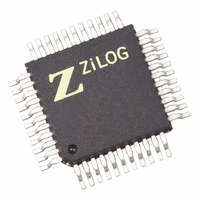
Z86E4312FSC Zilog, Z86E4312FSC Datasheet - Page 67

Z86E4312FSC
Manufacturer Part Number
Z86E4312FSC
Description
Z8 4K OTP 12 MHZ 44-PQFP
Manufacturer
Zilog
Series
Z8®r
Datasheet
1.Z86E3312SSC.pdf
(84 pages)
Specifications of Z86E4312FSC
Core Processor
Z8
Core Size
8-Bit
Speed
12MHz
Connectivity
EBI/EMI
Peripherals
POR, WDT
Number Of I /o
32
Program Memory Size
4KB (4K x 8)
Program Memory Type
OTP
Ram Size
236 x 8
Voltage - Supply (vcc/vdd)
3.5 V ~ 5.5 V
Oscillator Type
Internal
Operating Temperature
0°C ~ 70°C
Package / Case
44-LQFP
Data Bus Width
8 bit
Data Ram Size
236 B
Maximum Clock Frequency
12 MHz
Number Of Programmable I/os
32
Number Of Timers
2 bit
Operating Supply Voltage
3.5 V to 5.5 V
Maximum Operating Temperature
+ 70 C
Mounting Style
SMD/SMT
Minimum Operating Temperature
0 C
Lead Free Status / RoHS Status
Contains lead / RoHS non-compliant
Eeprom Size
-
Data Converters
-
Lead Free Status / Rohs Status
No
Other names
269-1108
Available stocks
Company
Part Number
Manufacturer
Quantity
Price
PS022901-0508
* Default setting after RESET
WDTMR (F) 0F
D7 D6 D5
Note:
WDTMR Register Accessibility. The WDTMR register is accessible only during the first
60 internal system clock cycles from the execution of the first instruction after Power-On
Reset, Watchdog reset or a Stop Mode Recovery
point, the register cannot be modified by any means, intentional or otherwise. The
WDTMR cannot be read and is located in Bank F of the Expanded Register File at address
location 0Fh.
Clock Free WDT Reset. The WDT will enable the Z8 to reset the I/0 pins whenever the
WDT times out, even without a clock source running on the XTAL1 and XTAL2 pins.
WDTMR Bit D4 must be 0 for the clock Free WDT to work. The I/O pins will default to
their default settings.
Figure 33. Watchdog Timer Mode Register Write Only
WDT time-out in STOP Mode will not reset SMR,SMR2,PCON,
WDTMR, P2M, P3M, Ports 2 & 3 Data Registers, but will activate
the T
D4 D3 D2 D1
POR
delay.
D0
WDT During HALT
0 OFF
1 ON*
WDT TAP
00
01*
10
11
WDT During STOP
0 OFF
1 ON*
XTAL1/INT RC Select for WDT
0 On-Board RC*
1 XTAL
Reserved (Must be 0)
INT RC OSC
10 ms
25 ms
80 ms
(Figure 33
5 ms
CMOS Z8
and
2048 TpC
External Clock
128 TpC
256 TpC
512 TpC
®
Product Specification
Figure
OTP Microcontrollers
Electrical Characteristics
34). After this
63


