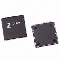
Z86C9620VSC Zilog, Z86C9620VSC Datasheet - Page 19

Z86C9620VSC
Manufacturer Part Number
Z86C9620VSC
Description
IC Z8 20MHZ C91 W/7 PORTS 68PLCC
Manufacturer
Zilog
Series
Z8®r
Datasheet
1.Z86C9620PSC.pdf
(42 pages)
Specifications of Z86C9620VSC
Core Processor
Z8
Core Size
8-Bit
Speed
20MHz
Connectivity
EBI/EMI, UART/USART
Number Of I /o
52
Program Memory Type
ROMless
Ram Size
236 x 8
Voltage - Supply (vcc/vdd)
3 V ~ 5.5 V
Oscillator Type
Internal
Operating Temperature
0°C ~ 70°C
Package / Case
68-PLCC
Lead Free Status / RoHS Status
Contains lead / RoHS non-compliant
Eeprom Size
-
Program Memory Size
-
Data Converters
-
Peripherals
-
Available stocks
Company
Part Number
Manufacturer
Quantity
Price
Company:
Part Number:
Z86C9620VSC
Manufacturer:
ZILOG
Quantity:
5 510
Company:
Part Number:
Z86C9620VSC
Manufacturer:
RURATEL
Quantity:
5 510
Part Number:
Z86C9620VSC
Manufacturer:
ZILOG
Quantity:
20 000
Zilog
PIN FUNCTIONS
R//RL (input, active Low). This pin when connected to
GND disables the internal ROM and forces the device to
function as a Z86C96 ROMless Z8. (Note: When left un-
connected or pulled High to VCC the part functions as a
normal Z86C61/62 ROM version.) This pin is only avail-
able on the 44-pin version of the Z86C61, and both ver-
sions of the Z86C62.
/DS (output, active Low). Data Strobe is activated once for
each external memory transfer. For a READ operation,
data must be available prior to the trailing edge of /DS. For
WRITE operations, the falling edge of /DS indicates that
output data is valid.
/AS (output, active Low). Address Strobe is pulsed once at
the beginning of each machine cycle. Address out-put is
through Port 1 for all external programs. Memory address
transfers are valid at the trailing edge of /AS. Under pro-
gram control, /AS can be placed in the high-impedance
state along with Ports 0 and 1, Data Strobe, and
Read/Write.
XTAL1, XTAL2 Crystal 1, Crystal 2 (time-based input and
output, respectively). These pins connect a parallel-reso-
nant crystal, ceramic resonator, LC, or any external single-
phase clock to the on-chip oscillator and buffer.
R//W (output, write Low). The Read/Write signal is Low
when the MCU is writing to the external program or data
memory.
/RESET (input, active Low). To avoid asynchronous and
noisy reset problems, the Z86C61/62/96 is equipped with
a reset filter of four external clocks (4TpC). If the external
/RESET signal is less than 4TpC in duration, no reset oc-
curs.
On the fifth clock after the /RESET is detected, an internal
RST signal is latched and held for an internal register
count of 18 external clocks, or for the duration of the exter-
nal /RESET, whichever is longer. During the reset cycle,
/DS is held active Low while /AS cycles at a rate of TpC/2.
When /RESET is deactivated, program execution begins
at location 000C (HEX). Reset time must be held Low for
50 ms, or until VCC is stable, whichever is longer.
DS97Z8X1600
PS003501-0301
P R E L I M I N A R Y
/P0DS Port 0 Data Strobe (output, active Low). Signal
used to emulate Port 0 when in ROMless mode.
/P1DS Port 1 Data Strobe (output, active Low). Signal
used to emulate Port 1 when in ROMless mode.
/DTIMERS Disable Timers (input, active Low). All timers
are stopped by the Low level at this pin. This pin has an in-
ternal pull up resistor.
SCLK (output). System clock pin.
/SYNC Instruction SYNC Signal (output, active Low). This
signal indicates the last clock of the current executing in-
struction.
Port 0 (P07-P00). Port 0 is an 8-bit, nibble programmable,
bidirectional, TTL compatible port. These eight I/O lines
can be configured under software control as a nibble I/O
port, or as an address port for interfacing external memory.
When used as an I/O port, Port 0 may be placed under
handshake control. In this configuration, Port 3, lines P32
and P35 are used as the handshake control /DAV0 and
RDY0 (Data Available and Ready). Handshake signal as-
signment is dictated by the I/O direction of the upper nibble
P07-P04. The lower nibble must have the same direction
as the upper nibble to be under handshake control.
For external memory references, Port 0 can provide ad-
dress bits A11-A8 (lower nibble) or A15-A8 (lower and up-
per nibble) depending on the required address space. If
the address range requires 12 bits or less, the upper nibble
of Port 0 can be programmed independently as I/O while
the lower nibble is used for addressing. If one or both nib-
bles are needed for I/O operation, they must be configured
by writing to the Port 0 Mode register.
In ROMless mode, after a hardware reset, Port 0 lines are
defined as address lines A15-A8, and extended timing is
set to accommodate slow memory access. The initializa-
tion routine includes reconfiguration to eliminate this ex-
tended timing mode (Figure 14).
CMOS Z8 Microcontroller
Z86C61/62/96
19
1


