EP7309-CVZ Cirrus Logic Inc, EP7309-CVZ Datasheet - Page 32
EP7309-CVZ
Manufacturer Part Number
EP7309-CVZ
Description
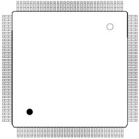
IC ARM720T MCU 74MHZ 208-LQFP
Manufacturer
Cirrus Logic Inc
Series
EP7r
Specifications of EP7309-CVZ
Core Size
32-Bit
Core Processor
ARM7
Speed
74MHz
Connectivity
Codec, DAI, EBI/EMI, IrDA, Keypad, SPI/Microwire1, UART/USART
Peripherals
LCD, LED, MaverickKey, POR, PWM
Number Of I /o
27
Program Memory Type
ROMless
Ram Size
56K x 8
Voltage - Supply (vcc/vdd)
2.3 V ~ 2.7 V
Oscillator Type
External
Operating Temperature
0°C ~ 70°C
Package / Case
208-LQFP
Controller Family/series
(ARM7)
No. Of I/o's
27
Ram Memory Size
48KB
Cpu Speed
74MHz
No. Of Timers
2
No. Of Pwm Channels
2
Digital Ic Case Style
LQFP
Embedded Interface Type
SSI, UART
Rohs Compliant
Yes
Processor Series
EP73xx
Core
ARM720T
Data Bus Width
32 bit
Mounting Style
SMD/SMT
3rd Party Development Tools
MDK-ARM, RL-ARM, ULINK2
Lead Free Status / RoHS Status
Lead free / RoHS Compliant
Eeprom Size
-
Program Memory Size
-
Data Converters
-
Lead Free Status / Rohs Status
Details
Other names
598-1214
Available stocks
Company
Part Number
Manufacturer
Quantity
Price


EP7309
High-Performance, Low-Power System on Chip
32
Ball Location
H10
H11
H12
H13
H14
H15
H16
K10
K12
K13
K14
K15
K16
J10
J11
J12
J13
J14
J15
J16
K11
H6
H7
H8
H9
K1
K2
K3
K4
K5
K6
K7
K8
K9
J1
J2
J3
J4
J5
J6
J7
J8
J9
L1
L2
L3
L4
L5
Table 20. 256-Ball PBGA Ball Listing (Continued)
PB[0]/PRDY[1]
PE[2]/CLKSEL
nTEST[1]
VSSRTC
VSSRTC
VSSRTC
VSSRTC
LEDDRV
VSSRTC
nEINT[1]
EINT[3]
TXD[1]
nTRST
ADCIN
COL[4]
VDDIO
VDDIO
RXD[1]
VDDIO
VSSIO
VSSIO
PHDIN
VSSIO
VSSIO
Name
TCLK
PB[2]
A[10]
A[12]
A[13]
D[14]
D[15]
PA[3]
PA[1]
PA[2]
PA[0]
A[17]
A[16]
A[15]
A[14]
D[16]
D[17]
D[20]
D[19]
D[18]
A[11]
DCD
DSR
CTS
RTC ground Real time clock ground
RTC ground Real time clock ground
RTC ground Real time clock ground
RTC ground Real time clock ground
RTC ground Real time clock ground
Pad ground I/O ground
Pad ground I/O ground
Pad ground I/O ground
Pad ground I/O ground
Pad power
Pad power
Pad power
Type
I/O
I/O
I/O
I/O
I/O
I/O
I/O
O
O
O
O
O
O
O
O
O
O
O
I
I
I
I
I
I
I
I
I
I
I
I
I
I
I
I
I
I
GPIO port B / CL-PS6700 interface
signal
GPIO port B
System byte address
System byte address
System byte address
System byte address
Data I/O
Data I/O
UART 1 transmit data out
System byte address
System byte address
System byte address
System byte address
Data I/O
Data I/O
UART 1 data carrier detect
SSI1 ADC serial input
Keyboard scanner column drive
JTAG clock
Data I/O
Data I/O
Data I/O
UART 1 receive data input
UART 1 data set ready input
GPIO port E / clock input mode select
GPIO port A
GPIO port A
GPIO port A
GPIO port A
UART 1 clear to send input
JTAG async reset input
IR LED drivet
Photodiode input
Test mode select input
External interrupt
Digital I/O power, 3.3V
Digital I/O power, 3.3V
Digital I/O power, 3.3V
External interrupt input
Description
Copyright Cirrus Logic, Inc. 2011
(All Rights Reserved)
Ball Location
M10
M12
M13
M14
M15
M16
M11
N10
N11
N12
N13
N14
N15
N16
L10
L11
L12
L13
L14
L15
L16
M1
M2
M3
M4
M5
M6
M7
M8
M9
L6
L7
L8
L9
N1
N2
N3
N4
N5
N6
N7
N8
N9
P1
P2
P3
P4
P5
Table 20. 256-Ball PBGA Ball Listing (Continued)
PE[0]/BOOTSEL[0]
PE[1]/BOOTSEL[1]
PD[0]/LEDFLSH
HALFWORD
SSIRXDA
nTEST[0]
SSITXFR
DRIVE[1]
nEXTFIQ
SMPCLK
RTCOUT
VSSRTC
VSSRTC
VSSRTC
nEINT[2]
ADCCLK
VSSRTC
COL[6]
VDDIO
VDDIO
COL[0]
VDDIO
VDDIO
COL[2]
VDDIO
VSSIO
VSSIO
VSSIO
VSSIO
VSSIO
VSSIO
Name
PD[5]
PD[2]
D[31]
A[22]
A[21]
A[18]
A[19]
FB[0]
D[27]
A[23]
A[20]
D[21]
D[29]
D[26]
D[22]
D[23]
TMS
RTC ground Real time clock ground
Core ground Real time clock ground
RTC ground Real time clock ground
RTC ground Real time clock ground
Pad ground I/O ground
Pad ground I/O ground
Pad ground I/O ground
Pad ground I/O ground
Pad ground I/O ground
Pad ground I/O ground
Pad power
Pad power
Pad power
Pad power
Pad power
Type
I/O
I/O
I/O
I/O
I/O
I/O
I/O
I/O
I/O
I/O
I/O
I/O
I/O
O
O
O
O
O
O
O
O
O
O
O
O
O
I
I
I
I
I
I
I
GPIO port D / LED blinker output
Keyboard scanner column drive
Data I/O
System byte address
System byte address
System byte address
System byte address
Test mode select input
External interrupt input
Digital I/O power, 3.3V
GPIO port E / Boot mode select
JTAG mode select
Digital I/O power, 3.3V
DAI/CODEC/SSI2 frame sync
PWM drive output
PWM feedback input
Keyboard scanner column drive
Data I/O
System byte address
Digital I/O power, 3.3V
System byte address
Data I/O
External fast interrupt input
GPIO port E / boot mode select
Digital I/O power, 3.3V
GPIO port D
GPIO port D
DAI/CODEC/SSI2 serial data input
SSI1 ADC serial clock
SSI1 ADC sample clock
Keyboard scanner column drive
Data I/O
Data I/O
Halfword access select output
Data I/O
Data I/O
Real time clock oscillator output
Digital I/O power, 3.3V
Description
DS507F2
Related parts for EP7309-CVZ
Image
Part Number
Description
Manufacturer
Datasheet
Request
R

Part Number:
Description:
IC ARM720T MCU 74MHZ 256-PBGA
Manufacturer:
Cirrus Logic Inc
Datasheet:

Part Number:
Description:
32-Bit Microcontroller IC
Manufacturer:
Cirrus Logic Inc
Datasheet:
Part Number:
Description:
IC, 32BIT MCU, ARM7, 74MHZ, BGA-256
Manufacturer:
Cirrus Logic Inc
Part Number:
Description:
IC, 32BIT MCU, ARM7, 74MHZ, LQFP-208
Manufacturer:
Cirrus Logic Inc

Part Number:
Description:
Development Kit
Manufacturer:
Cirrus Logic Inc
Datasheet:
Part Number:
Description:
Development Kit
Manufacturer:
Cirrus Logic Inc
Datasheet:


Part Number:
Description:
High-efficiency PFC + Fluorescent Lamp Driver Reference Design
Manufacturer:
Cirrus Logic Inc
Datasheet:
Part Number:
Description:
Development Kit
Manufacturer:
Cirrus Logic Inc
Datasheet:
Part Number:
Description:
Development Kit
Manufacturer:
Cirrus Logic Inc
Datasheet:

Part Number:
Description:
Development Kit
Manufacturer:
Cirrus Logic Inc
Datasheet:
Part Number:
Description:
Development Kit
Manufacturer:
Cirrus Logic Inc
Datasheet:

Part Number:
Description:
Ref Bd For Speakerbar MSA & DSP Products
Manufacturer:
Cirrus Logic Inc