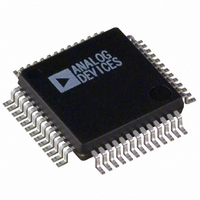
ADUC847BSZ8-3 Analog Devices Inc, ADUC847BSZ8-3 Datasheet - Page 7

ADUC847BSZ8-3
Manufacturer Part Number
ADUC847BSZ8-3
Description
IC MCU FLASH W/24BIT ADC 52MQFP
Manufacturer
Analog Devices Inc
Series
MicroConverter® ADuC8xxr
Datasheet
1.EVAL-ADUC845QSZ.pdf
(108 pages)
Specifications of ADUC847BSZ8-3
Core Size
8-Bit
Program Memory Size
8KB (8K x 8)
Core Processor
8052
Speed
12.58MHz
Connectivity
I²C, SPI, UART/USART
Peripherals
POR, PSM, PWM, Temp Sensor, WDT
Number Of I /o
34
Program Memory Type
FLASH
Eeprom Size
4K x 8
Ram Size
2.25K x 8
Voltage - Supply (vcc/vdd)
2.7 V ~ 3.6 V
Data Converters
A/D 10x24b; D/A 1x12b, 2x16b
Oscillator Type
Internal
Operating Temperature
-40°C ~ 125°C
Package / Case
52-MQFP, 52-PQFP
No. Of I/o's
32
Ram Memory Size
2.25KB
Cpu Speed
12MIPS
No. Of Timers
3
No. Of Pwm Channels
2
Digital Ic Case Style
QFP
Embedded Interface Type
I2C, SPI, UART
Rohs Compliant
Yes
Lead Free Status / RoHS Status
Lead free / RoHS Compliant
For Use With
EVAL-ADUC847QSZ - KIT DEV QUICK START FOR ADUC847
Lead Free Status / RoHS Status
Lead free / RoHS Compliant, Lead free / RoHS Compliant
Available stocks
Company
Part Number
Manufacturer
Quantity
Price
Company:
Part Number:
ADUC847BSZ8-3
Manufacturer:
Analog Devices Inc
Quantity:
10 000
Parameter
TRANSDUCER BURNOUT CURRENT
SOURCES
EXCITATION CURRENT SOURCES
POWER SUPPLY MONITOR (PSM)
CRYSTAL OSCILLATOR
(XTAL1 AND XTAL2)
LOGIC INPUTS
AIN+ Current
AIN− Current
Initial Tolerance at 25°C
Drift
Output Current
Initial Tolerance at 25°C
Drift
Initial Current Matching at 25°C
Drift Matching
Line Regulation (AV
Load Regulation
Output Compliance
AV
AV
DV
DV
Logic Inputs, XTAL1 Only
XTAL1 Input Capacitance
XTAL2 Output Capacitance
All inputs except SCLOCK, RESET,
and XTAL1
SCLOCK and RESET Only
(Schmidt Triggered Inputs)
Input Currents
Input Capacitance
V
V
V
V
V
V
V
Port 0, P1.0 to P1.7, EA
RESET
Port 2, Port 3
DD
DD
DD
DD
INL
INH
INL
INH
T+
T−
T+
Trip Point Selection Range
Trip Point Accuracy
Trip Point Selection Range
Trip Point Accuracy
, Input Low Voltage
, Input Low Voltage
− V
, Input Low Voltage
, Input Low Voltage
T−
2
DD
2
)
2
2
Min
AGND
2.63
2.63
3.5
2.5
2.0
1.3
0.95
0.8
0.4
0.3
35
−180
−20
Typ
−100
100
±10
0.03
200
±10
200
±1
20
1
0.1
18
18
10
Rev. B | Page 7 of 108
AV
DD
Max
4.63
±3.0
±4.0
4.63
±3.0
±4.0
0.8
0.4
0.8
0.4
3.0
2.5
1.4
1.1
0.85
±10
±10
105
±10
−660
−75
− 0.6
Unit
nA
nA
%/°C
µA
ppm/°C
%
µA/V
µA/V
V
pF
µA
µA
pF
%
%
ppm/°C
V
%
%
V
%
%
V
V
V
V
pF
V
V
V
V
V
V
V
V
µA
µA
µA
µA
Conditions
AIN+ is the selected positive input (AIN4 or AIN6
AIN− is the selected negative input (AIN5 or AIN7
Available from each current source
Matching between both current sources
AV
Four trip points selectable in this range
T
T
Four trip points selectable in this range
T
T
DV
DV
DV
DV
DV
DV
DV
DV
DV
DV
DV
V
V
V
V
V
V
All digital inputs
MAX
MAX
MAX
MAX
IN
IN
IN
IN
IN
IN
only) to the primary ADC
only) to the primary ADC
DD
DD
DD
DD
DD
DD
DD
DD
DD
DD
DD
DD
= 0 V or V
= 0 V, DV
= DV
= DV
= 2 V, DV
= 0.45 V, DV
ADuC845/ADuC847/ADuC848
= 85°C
= 125°C
= 85°C
= 125°C
= 5 V ± 5%
= 5 V
= 3 V
= 5 V
= 3 V
= 5 V
= 3 V
= 5 V
= 3 V
= 5 V
= 3 V
= 5 V or 3 V
DD
DD
, DV
, DV
DD
DD
DD
DD
DD
= 5 V
= 5 V
DD
= 5 V, internal pull-down
= 5 V
= 5 V


