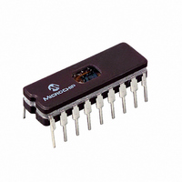
PIC16C558/JW Microchip Technology, PIC16C558/JW Datasheet - Page 25

PIC16C558/JW
Manufacturer Part Number
PIC16C558/JW
Description
IC MCU EPROM 2KX14 18CDIP
Manufacturer
Microchip Technology
Series
PIC® 16Cr
Specifications of PIC16C558/JW
Core Processor
PIC
Core Size
8-Bit
Speed
20MHz
Peripherals
POR, WDT
Number Of I /o
13
Program Memory Size
3.5KB (2K x 14)
Program Memory Type
EPROM, UV
Ram Size
128 x 8
Voltage - Supply (vcc/vdd)
2.5 V ~ 5.5 V
Oscillator Type
External
Operating Temperature
0°C ~ 70°C
Package / Case
18-CDIP (0.300", 7.62mm) Window
For Use With
ISPICR1 - ADAPTER IN-CIRCUIT PROGRAMMINGDVA16XP180 - ADAPTER DEVICE FOR MPLAB-ICEAC164010 - MODULE SKT PROMATEII DIP/SOIC
Lead Free Status / RoHS Status
Contains lead / RoHS non-compliant
Eeprom Size
-
Data Converters
-
Connectivity
-
Available stocks
Company
Part Number
Manufacturer
Quantity
Price
5.0
The PIC16C554 and PIC16C558 have two ports,
PORTA and PORTB. The PIC16C557 has three ports,
PORTA, PORTB and PORTC.
5.1
PORTA is a 5-bit wide latch. RA4 is a Schmitt Trigger
input and an open-drain output. Port RA4 is multiplexed
with the T0CKI clock input. All other RA port pins have
Schmitt Trigger input levels and full CMOS output driv-
ers. All pins have data direction bits (TRIS registers)
which can configure these pins as input or output.
A '1' in the TRISA register puts the corresponding out-
put driver in a Hi-impedance mode. A '0' in the TRISA
register puts the contents of the output latch on the
selected pin(s).
Reading the PORTA register reads the status of the
pins, whereas writing to it will write to the port latch. All
write operations are read-modify-write operations. So a
write to a port implies that the port pins are first read,
then this value is modified and written to the port data
latch.
FIGURE 5-1:
2002 Microchip Technology Inc.
WR
PORTA
Data
Bus
WR
TRISA
RD PORTA
Note 1: On RESET, the TRISA register is set to all
I/O PORTS
PORTA and TRISA Registers
Data Latch
TRIS Latch
inputs.
D
CK
D
CK
Q
Q
Q
Q
RD TRISA
BLOCK DIAGRAM OF
PORT PINS RA<3:0>
Q
Schmitt
Trigger
input
buffer
EN
D
V
V
P
N
SS
DD
V
V
DD
SS
I/O pin
Preliminary
FIGURE 5-2:
Data
bus
WR
TRISA
WR
PORTA
RD PORTA
TMR0 clock input
TRISA Latch
Data Latch
D
D
CK
CK
RD TRISA
Q
Q
Q
Q
BLOCK DIAGRAM OF RA4
PIN
PIC16C55X
Q
Schmitt
Trigger
input
buffer
EN
EN
D
DS40143D-page 23
V
N
SS
V
SS
I/O pin
(1)


