PIC17C756A-16/L Microchip Technology, PIC17C756A-16/L Datasheet - Page 140
PIC17C756A-16/L
Manufacturer Part Number
PIC17C756A-16/L
Description
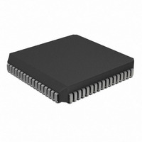
IC MCU OTP 16KX16 A/D PWM 68PLCC
Manufacturer
Microchip Technology
Series
PIC® 17Cr
Datasheets
1.PIC16F616T-ISL.pdf
(8 pages)
2.PIC17C752-16L.pdf
(304 pages)
3.PIC17C752-16L.pdf
(6 pages)
Specifications of PIC17C756A-16/L
Core Size
8-Bit
Program Memory Size
32KB (16K x 16)
Peripherals
Brown-out Detect/Reset, POR, PWM, WDT
Core Processor
PIC
Speed
16MHz
Connectivity
I²C, SPI, UART/USART
Number Of I /o
50
Program Memory Type
OTP
Ram Size
902 x 8
Voltage - Supply (vcc/vdd)
4.5 V ~ 5.5 V
Data Converters
A/D 12x10b
Oscillator Type
External
Operating Temperature
0°C ~ 70°C
Package / Case
68-PLCC
Controller Family/series
PIC17
No. Of I/o's
50
Ram Memory Size
902Byte
Cpu Speed
16MHz
No. Of Timers
4
Package
68PLCC
Device Core
PIC
Family Name
PIC17
Maximum Speed
16 MHz
Operating Supply Voltage
5 V
Data Bus Width
8 Bit
Number Of Programmable I/os
50
Interface Type
I2C/SPI/USART
On-chip Adc
12-chx10-bit
Number Of Timers
4
Processor Series
PIC17C
Core
PIC
Data Ram Size
902 B
Maximum Clock Frequency
33 MHz
Maximum Operating Temperature
+ 70 C
Mounting Style
SMD/SMT
Minimum Operating Temperature
0 C
Lead Free Status / RoHS Status
Lead free / RoHS Compliant
For Use With
AC164308 - MODULE SKT FOR PM3 68PLCCDVA17XL681 - DEVICE ADAPTER FOR PIC17C752DM173001 - KIT DEVELOPMENT PICDEM17AC174007 - MODULE SKT PROMATEII 68PLCCAC164024 - ADAPTER PICSTART PLUS 68PLCC
Eeprom Size
-
Lead Free Status / Rohs Status
Details
Available stocks
Company
Part Number
Manufacturer
Quantity
Price
Company:

Part Number:
PIC17C756A-16/L
Manufacturer:
MICROCHIP
Quantity:
101
Company:
Part Number:
PIC17C756A-16/L
Manufacturer:
Microchip Technology
Quantity:
10 000
Part Number:
PIC17C756A-16/L
Manufacturer:
MICROCHIP/微芯
Quantity:
20 000


PIC17C7XX
15.1.5
In Slave mode, the data is transmitted and received as
the external clock pulses appear on SCK. When the
last bit is latched, the interrupt flag bit SSPIF (PIR2<7>)
is set.
While in Slave mode, the external clock is supplied by
the external clock source on the SCK pin. This external
clock must meet the minimum high and low times as
specified in the electrical specifications.
While in SLEEP mode, the slave can transmit/receive
data. When a byte is received, the device will wake-up
from SLEEP.
15.1.6
The SS pin allows a Synchronous Slave mode. The
SPI must be in Slave mode with SS pin control
enabled (SSPCON1<3:0> = 04h). The pin must not
be driven low for the SS pin to function as an input.
The RA2 Data Latch must be high. When the SS pin
is low, transmission and reception are enabled and
FIGURE 15-7:
DS30289B-page 140
SCK
(CKP = 0
CKE = 0)
SS
SCK
(CKP = 1
CKE = 0)
Write to
SSPBUF
SDO
SDI
(SMP = 0)
Input
Sample
(SMP = 0)
SSPIF
Interrupt
Flag
SSPSR to
SSPBUF
SLAVE MODE
SLAVE SELECT
SYNCHRONIZATION
SLAVE SYNCHRONIZATION WAVEFORM
bit7
bit7
bit6
the SDO pin is driven. When the SS pin goes high,
the SDO pin is no longer driven, even if in the mid-
dle of a transmitted byte and becomes a floating
output. External pull-up/pull-down resistors may be
desirable, depending on the application.
When the SPI module resets, the bit counter is forced
to 0. This can be done by either forcing the SS pin to a
high level, or clearing the SSPEN bit.
To emulate two-wire communication, the SDO pin can
be connected to the SDI pin. When the SPI needs to
operate as a receiver, the SDO pin can be configured
as an input. This disables transmissions from the SDO.
The SDI can always be left as an input (SDI function),
since it cannot create a bus conflict.
Note 1: When the SPI is in Slave mode with SS
2: If the SPI is used in Slave mode with
pin control enabled (SSPCON<3:0> =
0100), the SPI module will reset if the SS
pin is set to V
CKE = ’1’, then the SS pin control must be
enabled.
bit7
bit7
DD
2000 Microchip Technology Inc.
.
Next Q4 cycle
after Q2
bit0
bit0
Related parts for PIC17C756A-16/L
Image
Part Number
Description
Manufacturer
Datasheet
Request
R

Part Number:
Description:
MICRO CTRL 16K MEMORY OTP 64SDIP
Manufacturer:
Microchip Technology
Datasheet:
Part Number:
Description:
MICRO CTRL 16K MEMORY OTP 64SDIP
Manufacturer:
Microchip Technology
Datasheet:
Part Number:
Description:
MICRO CTRL 16K MEMORY OTP 68PLCC
Manufacturer:
Microchip Technology
Datasheet:
Part Number:
Description:
MICRO CTRL 16K MEMORY OTP 68PLCC
Manufacturer:
Microchip Technology
Datasheet:
Part Number:
Description:
MICRO CTRL 16K MEMORY OTP 68PLCC
Manufacturer:
Microchip Technology
Datasheet:
Part Number:
Description:
MICRO CTRL 16K MEMORY OTP 64SDIP
Manufacturer:
Microchip Technology
Datasheet:
Part Number:
Description:
MICRO CTRL 16K MEMORY OTP 64SDIP
Manufacturer:
Microchip Technology
Datasheet:
Part Number:
Description:
MICRO CTRL 16K MEMORY EPROM 68CL
Manufacturer:
Microchip Technology
Datasheet:
Part Number:
Description:
MICRO CTRL 16K MEMORY OTP 68PLCC
Manufacturer:
Microchip Technology
Datasheet:
Part Number:
Description:
High-Performance 8-Bit CMOS EPROM Microcontrollers
Manufacturer:
Microchip Technology

Part Number:
Description:
Manufacturer:
Microchip Technology Inc.
Datasheet:
Part Number:
Description:
Manufacturer:
Microchip Technology Inc.
Datasheet:
Part Number:
Description:
Manufacturer:
Microchip Technology Inc.
Datasheet: