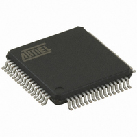
AT32UC3B0128-A2UT Atmel, AT32UC3B0128-A2UT Datasheet - Page 201

AT32UC3B0128-A2UT
Manufacturer Part Number
AT32UC3B0128-A2UT
Description
IC MCU AVR32 128KB FLASH 64-TQFP
Manufacturer
Atmel
Series
AVR®32 UC3r
Specifications of AT32UC3B0128-A2UT
Core Processor
AVR
Core Size
32-Bit
Speed
60MHz
Connectivity
I²C, IrDA, SPI, SSC, UART/USART, USB
Peripherals
Brown-out Detect/Reset, DMA, POR, PWM, WDT
Number Of I /o
44
Program Memory Size
128KB (128K x 8)
Program Memory Type
FLASH
Ram Size
32K x 8
Voltage - Supply (vcc/vdd)
1.65 V ~ 1.95 V
Data Converters
A/D 8x10b
Oscillator Type
Internal
Operating Temperature
-40°C ~ 85°C
Package / Case
64-TQFP, 64-VQFP
Processor Series
AT32UC3x
Core
AVR32
Data Bus Width
32 bit
Data Ram Size
32 KB
Interface Type
2-Wire, SPI, USART
Maximum Clock Frequency
60 MHz
Number Of Programmable I/os
44
Number Of Timers
3
Maximum Operating Temperature
+ 85 C
Mounting Style
SMD/SMT
3rd Party Development Tools
EWAVR32, EWAVR32-BL
Development Tools By Supplier
ATAVRDRAGON, ATSTK500, ATSTK600, ATAVRISP2, ATAVRONEKIT, ATEXTWIFI, ATEVK1101
Minimum Operating Temperature
- 40 C
On-chip Adc
10 bit, 8 Channel
Package
64TQFP
Device Core
AVR32
Family Name
AT32
Maximum Speed
60 MHz
Operating Supply Voltage
1.8|3.3 V
For Use With
ATAVRONEKIT - KIT AVR/AVR32 DEBUGGER/PROGRMMR770-1008 - ISP 4PORT ATMEL AVR32 MCU SPIATSTK600-TQFP64-2 - STK600 SOCKET/ADAPTER FOR 64-TQFATEVK1101 - KIT DEV/EVAL FOR AVR32 AT32UC3B
Lead Free Status / RoHS Status
Lead free / RoHS Compliant
Eeprom Size
-
Lead Free Status / Rohs Status
Details
Available stocks
Company
Part Number
Manufacturer
Quantity
Price
Company:
Part Number:
AT32UC3B0128-A2UT
Manufacturer:
XILINX
Quantity:
150
- Current page: 201 of 692
- Download datasheet (11Mb)
18.7.3.3
18.7.3.4
Figure 18-7. Programmable Delays
32059K–03/2011
Chip Select 1
Chip Select 2
Clock Generation
Transfer Delays
SPCK
The SPI Baud rate clock is generated by dividing the CLK_SPI by a value between 1 and 255.
This allows a maximum operating baud rate at up to CLK_SPI and a minimum operating baud
rate of CLK_SPI divided by 255.
Programming the SCBR field at 0 is forbidden. Triggering a transfer while SCBR is at 0 can lead
to unpredictable results.
At reset, SCBR is 0 and the user has to program it at a valid value before performing the first
transfer.
The divisor can be defined independently for each chip select, as it has to be programmed in the
SCBR field of the Chip Select Registers. This allows the SPI to automatically adapt the baud
rate for each interfaced peripheral without reprogramming.
Figure 18-7 on page 201
same chip select. Three delays can be programmed to modify the transfer waveforms:
These delays allow the SPI to be adapted to the interfaced peripherals and their speed and bus
release time.
• The delay between chip selects, programmable only once for all the chip selects by writing
• The delay before SPCK, independently programmable for each chip select by writing the field
• The delay between consecutive transfers, independently programmable for each chip select
the DLYBCS field in the Mode Register. Allows insertion of a delay between release of one
chip select and before assertion of a new one.
DLYBS. Allows the start of SPCK to be delayed after the chip select has been asserted.
by writing the DLYBCT field. Allows insertion of a delay between two transfers occurring on
the same chip select
DLYBCS
DLYBS
shows a chip select transfer change and consecutive transfers on the
DLYBCT
AT32UC3B
DLYBCT
201
Related parts for AT32UC3B0128-A2UT
Image
Part Number
Description
Manufacturer
Datasheet
Request
R

Part Number:
Description:
DEV KIT FOR AVR/AVR32
Manufacturer:
Atmel
Datasheet:

Part Number:
Description:
INTERVAL AND WIPE/WASH WIPER CONTROL IC WITH DELAY
Manufacturer:
ATMEL Corporation
Datasheet:

Part Number:
Description:
Low-Voltage Voice-Switched IC for Hands-Free Operation
Manufacturer:
ATMEL Corporation
Datasheet:

Part Number:
Description:
MONOLITHIC INTEGRATED FEATUREPHONE CIRCUIT
Manufacturer:
ATMEL Corporation
Datasheet:

Part Number:
Description:
AM-FM Receiver IC U4255BM-M
Manufacturer:
ATMEL Corporation
Datasheet:

Part Number:
Description:
Monolithic Integrated Feature Phone Circuit
Manufacturer:
ATMEL Corporation
Datasheet:

Part Number:
Description:
Multistandard Video-IF and Quasi Parallel Sound Processing
Manufacturer:
ATMEL Corporation
Datasheet:

Part Number:
Description:
High-performance EE PLD
Manufacturer:
ATMEL Corporation
Datasheet:

Part Number:
Description:
8-bit Flash Microcontroller
Manufacturer:
ATMEL Corporation
Datasheet:

Part Number:
Description:
2-Wire Serial EEPROM
Manufacturer:
ATMEL Corporation
Datasheet:


