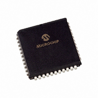
PIC18C452-E/L Microchip Technology, PIC18C452-E/L Datasheet - Page 2

PIC18C452-E/L
Manufacturer Part Number
PIC18C452-E/L
Description
IC MCU OTP 16KX16 A/D 44PLCC
Manufacturer
Microchip Technology
Series
PIC® 18Cr
Datasheets
1.PIC16F616T-ISL.pdf
(8 pages)
2.PIC16C770-ISO.pdf
(8 pages)
3.PIC18C242-ISO.pdf
(305 pages)
4.PIC18C242-ISO.pdf
(12 pages)
Specifications of PIC18C452-E/L
Core Processor
PIC
Core Size
8-Bit
Speed
40MHz
Connectivity
I²C, SPI, UART/USART
Peripherals
Brown-out Detect/Reset, LVD, POR, PWM, WDT
Number Of I /o
33
Program Memory Size
32KB (16K x 16)
Program Memory Type
OTP
Ram Size
1.5K x 8
Voltage - Supply (vcc/vdd)
4.2 V ~ 5.5 V
Data Converters
A/D 8x10b
Oscillator Type
External
Operating Temperature
-40°C ~ 125°C
Package / Case
44-PLCC
Processor Series
PIC18C
Core
PIC
Data Bus Width
8 bit
Data Ram Size
1.5 KB
Interface Type
MSSP, SPI, I2C, PSP, USART
Maximum Clock Frequency
40 MHz
Number Of Programmable I/os
34
Number Of Timers
1 x 16 bit
Operating Supply Voltage
2.5 V to 5.5 V
Maximum Operating Temperature
+ 125 C
Mounting Style
SMD/SMT
3rd Party Development Tools
52715-96, 52716-328, 52717-734, 52712-325, EWPIC18
Development Tools By Supplier
ICE2000, DM163022, DV164136
Minimum Operating Temperature
- 40 C
On-chip Adc
8
For Use With
I3DB18C452 - BOARD DAUGHTER ICEPIC3DVA16XL441 - ADAPTER DEVICE ICE 44PLCC
Lead Free Status / RoHS Status
Lead free / RoHS Compliant
Eeprom Size
-
Lead Free Status / Rohs Status
Details
Other names
PIC18C452E/L
Available stocks
Company
Part Number
Manufacturer
Quantity
Price
Company:
Part Number:
PIC18C452-E/L
Manufacturer:
Microchip Technology
Quantity:
10 000
PIC18CXX2
4. Module: CCP (Compare Mode)
TABLE 1:
DS80058H-page 2
CCPxM<3:0> =
The Compare mode may not operate as expected
when configuring the compare match to drive the
I/O pin low (CCPxM<3:0> = 1001).
When the CCP module is changed to compare
output low (CCPxM<3:0> = 1001) from any other
non-compare CCP mode, the I/O pin will immedi-
ately be driven low, regardless of the state of the
I/O data latch. The pin will remain low when the
compare match occurs (see Table 1).
However, when the CCP module is changed to
compare output high (CCPxM<3:0> = 1000) from
any other CCP mode, the I/O pin will immediately
be driven low, regardless of the state of the I/O
data latch. The pin will be driven high when the
compare match occurs.
Work around
To have the I/O pin high until the compare match
low occurs, force a compare match high to get the
I/O pin into the high state, then reconfigure the
compare match to force the I/O low when the
compare condition occurs.
CCP Mode
0xxx
1000
1001
101x
11xx
COMPARE OUTPUT LOW
SWITCHING
I/O Pin
State
H
H
H
H
H
L
L
L
L
L
Change CCP to
CCPxM<3:0> =
1001
—
—
H
L
L
L
L
L
L
L
1000
—
—
L
L
L
L
L
L
L
L
5. Module: Timer1 and Timer3
6. Module: I/O (Parallel Slave Port)
When the prescaler select bits (bits 5:4 of the
T1CON or T3CON registers) are modified, the
timer may inadvertently increment. This can occur
even if the timer is in the OFF state. Changing the
prescaler may cause clock glitches, which may
cause the counter to increment improperly.
Work around
Always re-initialize the timer registers (either
TMR1H and TMR1L, or TMR3H and TMR3L) after
changing the prescaler bits of registers T1CON or
T3CON.
As an alternative, store the timer value before chang-
ing the prescaler bits of the timer control registers,
and restore the timer value after changing the bits.
The Input Buffer Status bit of the TRISE register
(TRISE<7>) may be inadvertently cleared, even
when the PORTE input buffer has not been read.
This will occur only when the following two condi-
tions occur simultaneously:
•
•
Work around
All work arounds will involve setting the contents of
BSR<3:0> to some value other than 0Fh. In addition
to those proposed below, other solutions may exist.
1. When developing or modifying code, keep
2. If accessing a part of Bank 15 is required and
3. If pointing the BSR to Bank 15 is unavoidable,
The four Least Significant bits of the BSR
register are equal to 0Fh
(BSR<3:0> = ‘1111’), and
Any instruction that contains 83h in its 8
Least Significant bits (i.e., register file
addresses, literal data, address offsets,
etc.) is executed.
these guidelines in mind:
•
•
•
the use of Access Banking is not possible,
consider using indirect addressing.
review the absolute file listing. Verify that no
instructions contains 83h in the 8 Least Signif-
icant bits while the BSR points to Bank 15
(BSR = 0Fh).
Assign 12-bit addresses to all variables.
This allows the assembler to know when
Access Banking can be used.
Do not set the BSR to point to Bank 15
(BSR = 0Fh).
Allow the assembler to manipulate the
Access bit present in most instructions.
Accessing the SFRs in Bank 15 will be
done through the Access Bank. Con-
tinue to use the BSR to select Banks 1
through 5 and the upper half of Bank 0.
2002 Microchip Technology Inc.


