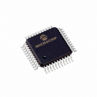
PIC17C42A-25/PQ Microchip Technology, PIC17C42A-25/PQ Datasheet - Page 113

PIC17C42A-25/PQ
Manufacturer Part Number
PIC17C42A-25/PQ
Description
IC MCU OTP 2KX16 PWM 44-MQFP
Manufacturer
Microchip Technology
Series
PIC® 17Cr
Datasheets
1.PIC16F616T-ISL.pdf
(8 pages)
2.PIC17C42A-16P.pdf
(241 pages)
3.PIC17C42A-16P.pdf
(4 pages)
Specifications of PIC17C42A-25/PQ
Core Processor
PIC
Core Size
8-Bit
Speed
25MHz
Connectivity
UART/USART
Peripherals
POR, PWM, WDT
Number Of I /o
33
Program Memory Size
4KB (2K x 16)
Program Memory Type
OTP
Ram Size
232 x 8
Voltage - Supply (vcc/vdd)
4.5 V ~ 6 V
Oscillator Type
External
Operating Temperature
0°C ~ 70°C
Package / Case
44-MQFP, 44-PQFP
Processor Series
PIC17C
Core
PIC
Data Bus Width
8 bit
Data Ram Size
232 B
Interface Type
SCI, USART
Maximum Clock Frequency
25 MHz
Number Of Programmable I/os
33
Number Of Timers
8
Operating Supply Voltage
2.5 V to 6 V
Maximum Operating Temperature
+ 70 C
Mounting Style
SMD/SMT
Development Tools By Supplier
ICE2000
Minimum Operating Temperature
0 C
For Use With
AC164316 - MODULE SKT MPLAB PM3 44MQFP
Lead Free Status / RoHS Status
Lead free / RoHS Compliant
Eeprom Size
-
Data Converters
-
Lead Free Status / Rohs Status
Details
Available stocks
Company
Part Number
Manufacturer
Quantity
Price
Company:
Part Number:
PIC17C42A-25/PQ
Manufacturer:
Microchip Technology
Quantity:
10 000
- Current page: 113 of 241
- Download datasheet (2Mb)
ADDWFC
Syntax:
Operands:
Operation:
Status Affected:
Encoding:
Description:
Words:
Cycles:
Q Cycle Activity:
Example:
1996 Microchip Technology Inc.
Before Instruction
After Instruction
Decode
Carry bit =
REG
WREG
Carry bit =
REG
WREG
Q1
=
=
=
=
register 'f'
ADD WREG and Carry bit to f
[ label ] ADDWFC
0
d
(WREG) + (f) + C
Add WREG, the Carry Flag and data
memory location 'f'. If 'd' is 0, the result is
placed in WREG. If 'd' is 1, the result is
placed in data memory location 'f'.
1
1
ADDWFC
OV, C, DC, Z
Read
Q2
0001
1
0x02
0x4D
0
0x02
0x50
f
255
000d
REG
Execute
Q3
0
f,d
(dest)
ffff
destination
Write to
Q4
ffff
ANDLW
Syntax:
Operands:
Operation:
Status Affected:
Encoding:
Description:
Words:
Cycles:
Q Cycle Activity:
Example:
Before Instruction
After Instruction
Decode
WREG
WREG
Q1
=
=
Read literal
And Literal with WREG
[ label ] ANDLW
0
(WREG) .AND. (k)
Z
The contents of WREG are AND’ed with
the 8-bit literal 'k'. The result is placed in
WREG.
1
1
ANDLW
1011
Q2
'k'
0xA3
0x03
k
255
PIC17C4X
0101
0x5F
Execute
Q3
DS30412C-page 113
k
kkkk
(WREG)
Write to
WREG
Q4
kkkk
Related parts for PIC17C42A-25/PQ
Image
Part Number
Description
Manufacturer
Datasheet
Request
R

Part Number:
Description:
IC,MICROCONTROLLER,8-BIT,PIC CPU,CMOS,LDCC,44PIN,PLASTIC
Manufacturer:
Microchip Technology
Datasheet:

Part Number:
Description:
IC MCU OTP 2KX16 PWM 40DIP
Manufacturer:
Microchip Technology
Datasheet:

Part Number:
Description:
IC MCU OTP 2KX16 PWM 40DIP
Manufacturer:
Microchip Technology
Datasheet:

Part Number:
Description:
IC MCU OTP 2KX16 PWM 44PLCC
Manufacturer:
Microchip Technology
Datasheet:

Part Number:
Description:
IC MCU OTP 2KX16 PWM 44PLCC
Manufacturer:
Microchip Technology
Datasheet:

Part Number:
Description:
IC MCU OTP 2KX16 PWM 44-MQFP
Manufacturer:
Microchip Technology
Datasheet:

Part Number:
Description:
IC MCU OTP 2KX16 PWM 44TQFP
Manufacturer:
Microchip Technology
Datasheet:

Part Number:
Description:
IC MCU OTP 2KX16 PWM 44-MQFP
Manufacturer:
Microchip Technology
Datasheet:

Part Number:
Description:
IC MCU OTP 2KX16 PWM 44TQFP
Manufacturer:
Microchip Technology
Datasheet:

Part Number:
Description:
IC MCU OTP 2KX16 PWM 40DIP
Manufacturer:
Microchip Technology
Datasheet:

Part Number:
Description:
IC MCU OTP 2KX16 PWM 40DIP
Manufacturer:
Microchip Technology
Datasheet:

Part Number:
Description:
IC MCU OTP 2KX16 PWM 40DIP
Manufacturer:
Microchip Technology
Datasheet:

Part Number:
Description:
IC MCU OTP 2KX16 PWM 44-MQFP
Manufacturer:
Microchip Technology
Datasheet:

Part Number:
Description:
IC MCU OTP 2KX16 PWM 44PLCC
Manufacturer:
Microchip Technology
Datasheet:

Part Number:
Description:
IC MCU OTP 2KX16 PWM 44-MQFP
Manufacturer:
Microchip Technology
Datasheet:


