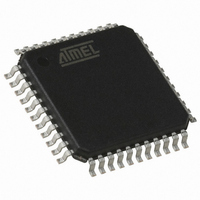
AT89C51RD2-RLRUM Atmel, AT89C51RD2-RLRUM Datasheet - Page 18

AT89C51RD2-RLRUM
Manufacturer Part Number
AT89C51RD2-RLRUM
Description
IC MCU FLASH 8051 EEP 64K 44VQFP
Manufacturer
Atmel
Series
89Cr
Datasheet
1.ATWEBDVK-02RC.pdf
(137 pages)
Specifications of AT89C51RD2-RLRUM
Core Processor
8051
Core Size
8-Bit
Speed
60MHz
Connectivity
SPI, UART/USART
Peripherals
POR, PWM, WDT
Number Of I /o
34
Program Memory Size
64KB (64K x 8)
Program Memory Type
FLASH
Ram Size
2K x 8
Voltage - Supply (vcc/vdd)
2.7 V ~ 5.5 V
Oscillator Type
External
Operating Temperature
-40°C ~ 85°C
Package / Case
44-TQFP, 44-VQFP
Processor Series
AT89x
Core
8051
Data Bus Width
8 bit
Data Ram Size
2 KB
Interface Type
UART, SPI
Maximum Clock Frequency
60 MHz
Number Of Programmable I/os
32
Number Of Timers
3
Operating Supply Voltage
2.7 V to 5.5 V
Mounting Style
SMD/SMT
3rd Party Development Tools
PK51, CA51, A51, ULINK2
For Use With
AT89STK-11 - KIT STARTER FOR AT89C51RX2
Lead Free Status / RoHS Status
Lead free / RoHS Compliant
Eeprom Size
-
Data Converters
-
Lead Free Status / Rohs Status
Details
Other names
AT89C51RD2-RLRUMTR
Available stocks
Company
Part Number
Manufacturer
Quantity
Price
Company:
Part Number:
AT89C51RD2-RLRUM
Manufacturer:
ATMEL
Quantity:
101
Figure 7-2.
18
AT89C51RD2/ED2
XTAL1
XTAL1:2
X2 Bit
CPU Clock
Mode Switching Waveforms
STD Mode
Figure 7-1.
The X2 bit in the CKCON0 register (see Table 7-1) allows a switch from 12 clock periods per
instruction to 6 clock periods and vice versa. At reset, the speed is set according to X2 bit of
Hardware Security Byte (HSB). By default, Standard mode is active. Setting the X2 bit activates
the X2 feature (X2 mode).
The T0X2, T1X2, T2X2, UartX2, PcaX2, and WdX2 bits in the CKCON0 register
SPIX2 bit in the CKCON1 register (see Table 7-2) allows a switch from standard peripheral
speed (12 clock periods per peripheral clock cycle) to fast peripheral speed (6 clock periods per
peripheral clock cycle). These bits are active only in X2 mode.
Table 7-1.
CKCON0 - Clock Control Register (8Fh)
Number
Bit
7
7
6
-
XTAL1
Mnemonic
Reserved
Clock Generation Diagram
CKCON0 Register
WDX2
WDX2
Bit
6
FXTAL
Description
The values for this bit are indeterminite. Do not set this bit.
Watchdog Clock
(This control bit is validated when the CPU clock X2 is set; when X2 is low, this bit has no
effect).
Cleared to select 6 clock periods per peripheral clock cycle.
Set to select 12 clock periods per peripheral clock cycle.
PCAX2
5
2
F
XTAL1:2
X2 Mode
OSC
SIX2
4
CKCON0
X2
0
1
F
OSC
T2X2
3
8-bit Prescaler
CKRL
T1X2
2
STD Mode
T0X2
1
(Table
4235K–8051–05/08
F
F
CLK CPU
CLK PERIPH
7-1) and
X2
0


