PIC18LF47J53-I/ML Microchip Technology, PIC18LF47J53-I/ML Datasheet - Page 106
PIC18LF47J53-I/ML
Manufacturer Part Number
PIC18LF47J53-I/ML
Description
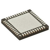
IC PIC MCU 128KB FLASH 44QFN
Manufacturer
Microchip Technology
Series
PIC® XLP™ 18Fr
Datasheets
1.PIC18LF24J10-ISS.pdf
(32 pages)
2.PIC18F26J13-ISS.pdf
(496 pages)
3.PIC18F26J53-ISS.pdf
(586 pages)
4.PIC18F26J53-ISS.pdf
(12 pages)
Specifications of PIC18LF47J53-I/ML
Core Size
8-Bit
Program Memory Size
128KB (64K x 16)
Core Processor
PIC
Speed
48MHz
Connectivity
I²C, LIN, SPI, UART/USART, USB
Peripherals
Brown-out Detect/Reset, POR, PWM, WDT
Number Of I /o
34
Program Memory Type
FLASH
Ram Size
3.8K x 8
Voltage - Supply (vcc/vdd)
2 V ~ 2.75 V
Data Converters
A/D 13x10b/12b
Oscillator Type
Internal
Operating Temperature
-40°C ~ 85°C
Package / Case
*
Controller Family/series
PIC18
Cpu Speed
48MHz
Digital Ic Case Style
QFN
Supply Voltage Range
1.8V To 3.6V
Embedded Interface Type
I2C, SPI, USART
Rohs Compliant
Yes
Lead Free Status / RoHS Status
Lead free / RoHS Compliant
Eeprom Size
-
Lead Free Status / RoHS Status
Lead free / RoHS Compliant, Lead free / RoHS Compliant


PIC18(L)F2X/4XK22
REGISTER 7-1:
DS41412D-page 106
bit 7
Legend:
R = Readable bit
S = Bit can be set by software, but not cleared
-n = Value at POR
bit 7
bit 6
bit 5
bit 4
bit 3
bit 2
bit 1
bit 0
Note 1:
EEPGD
R/W-x
When a WRERR occurs, the EEPGD and CFGS bits are not cleared. This allows tracing of the
error condition.
EEPGD: Flash Program or Data EEPROM Memory Select bit
1 = Access Flash program memory
0 = Access data EEPROM memory
CFGS: Flash Program/Data EEPROM or Configuration Select bit
1 = Access Configuration registers
0 = Access Flash program or data EEPROM memory
Unimplemented: Read as ‘0’
FREE: Flash Row (Block) Erase Enable bit
1 = Erase the program memory block addressed by TBLPTR on the next WR command
0 = Perform write-only
WRERR: Flash Program/Data EEPROM Error Flag bit
1 = A write operation is prematurely terminated (any Reset during self-timed programming in normal
0 = The write operation completed
WREN: Flash Program/Data EEPROM Write Enable bit
1 = Allows write cycles to Flash program/data EEPROM
0 = Inhibits write cycles to Flash program/data EEPROM
WR: Write Control bit
1 = Initiates a data EEPROM erase/write cycle or a program memory erase cycle or write cycle.
0 = Write cycle to the EEPROM is complete
RD: Read Control bit
1 = Initiates an EEPROM read (Read takes one cycle. RD is cleared by hardware. The RD bit can only
0 = Does not initiate an EEPROM read
R/W-x
CFGS
(cleared by completion of erase operation)
operation, or an improper write attempt)
(The operation is self-timed and the bit is cleared by hardware once write is complete.
The WR bit can only be set (not cleared) by software.)
be set (not cleared) by software. RD bit cannot be set when EEPGD = 1 or CFGS = 1.)
EECON1: DATA EEPROM CONTROL 1 REGISTER
W = Writable bit
‘1’ = Bit is set
U-0
—
R/W-0
FREE
Preliminary
U = Unimplemented bit, read as ‘0’
‘0’ = Bit is cleared
WRERR
R/W-x
(1)
WREN
R/W-0
2010 Microchip Technology Inc.
x = Bit is unknown
R/S-0
WR
R/S-0
RD
bit 0
Related parts for PIC18LF47J53-I/ML
Image
Part Number
Description
Manufacturer
Datasheet
Request
R

Part Number:
Description:
Manufacturer:
Microchip Technology Inc.
Datasheet:
Part Number:
Description:
Manufacturer:
Microchip Technology Inc.
Datasheet:
Part Number:
Description:
Manufacturer:
Microchip Technology Inc.
Datasheet:
Part Number:
Description:
Manufacturer:
Microchip Technology Inc.
Datasheet:
Part Number:
Description:
Manufacturer:
Microchip Technology Inc.
Datasheet:
Part Number:
Description:
Manufacturer:
Microchip Technology Inc.
Datasheet:
Part Number:
Description:
Manufacturer:
Microchip Technology Inc.
Datasheet:
Part Number:
Description:
Manufacturer:
Microchip Technology Inc.
Datasheet: