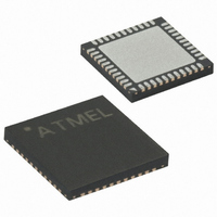
ATXMEGA16D4-MH Atmel, ATXMEGA16D4-MH Datasheet - Page 12

ATXMEGA16D4-MH
Manufacturer Part Number
ATXMEGA16D4-MH
Description
MCU AVR 16KB FLASH 44VQFN
Manufacturer
Atmel
Series
AVR® XMEGAr
Datasheet
1.ATXMEGA16D4-AU.pdf
(105 pages)
Specifications of ATXMEGA16D4-MH
Core Processor
AVR
Core Size
8/16-Bit
Speed
32MHz
Connectivity
I²C, IrDA, SPI, UART/USART
Peripherals
Brown-out Detect/Reset, POR, PWM, WDT
Number Of I /o
34
Program Memory Size
16KB (8K x 16)
Program Memory Type
FLASH
Eeprom Size
1K x 8
Ram Size
2K x 8
Voltage - Supply (vcc/vdd)
1.6 V ~ 3.6 V
Data Converters
A/D 12x12b
Oscillator Type
Internal
Operating Temperature
-40°C ~ 85°C
Package / Case
44-VQFN Exposed Pad
Processor Series
XMEGA
Core
AVR
Data Bus Width
8 bit, 16 bit
Data Ram Size
2 KB
Interface Type
SPI, USART
Maximum Clock Frequency
32 MHz
Number Of Programmable I/os
34
Number Of Timers
4
Operating Supply Voltage
2.5 V
Maximum Operating Temperature
+ 85 C
Mounting Style
SMD/SMT
3rd Party Development Tools
EWAVR, EWAVR-BL
Minimum Operating Temperature
- 40 C
Operating Temperature Range
- 40 C to + 85 C
Lead Free Status / RoHS Status
Lead free / RoHS Compliant
Available stocks
Company
Part Number
Manufacturer
Quantity
Price
Company:
Part Number:
ATXMEGA16D4-MH
Manufacturer:
Atmel
Quantity:
1 605
Company:
Part Number:
ATXMEGA16D4-MHR
Manufacturer:
SANYO
Quantity:
50
Part Number:
ATXMEGA16D4-MHR
Manufacturer:
ATMEL/爱特梅尔
Quantity:
20 000
7.4
Figure 7-2.
7.4.1
7.4.2
8135J–AVR–12/10
Byte Address
Data Memory
I/O Memory
SRAM Data Memory
2FFF
17FF
1000
2000
FFF
Data Memory Map (Hexadecimal address)
0
ATxmega64D4
Internal SRAM
I/O Registers
RESERVED
EEPROM
(4 KB)
(4KB)
(2K)
The Data Memory containts the I/O Memory, EEPROM and SRAM memories, all within one lin-
ear address space, see
devices in the family is identical and with empty, reserved memory space for smaller devices.
All peripherals and modules are addressable through I/O memory locations in the data memory
space. All I/O memory locations can be accessed by the Load (LD/LDS/LDD) and Store
(ST/STS/STD) instructions, transferring data between the 32 general purpose registers in the
CPU and the I/O Memory.
The IN and OUT instructions can address I/O memory locations in the range 0x00 - 0x3F
directly.
I/O registers within the address range 0x00 - 0x1F are directly bit-accessible using the SBI and
CBI instructions. The value of single bits can be checked by using the SBIS and SBIC instruc-
tions on these registers.
The I/O memory address for all peripherals and modules in XMEGA D4 is shown in the
eral Module Address Map” on page
The XMEGA D4 devices have internal SRAM memory for data storage.
Byte Address
Figure 7-2 on page
2FFF
13FF
1000
2000
FFF
0
50.
ATxmega32D4
Internal SRAM
I/O Registers
RESERVED
EEPROM
(1 KB)
(4 KB)
(4KB)
12. To simplify development, the memory map for all
Byte Address
Byte Address
3FFF
17FF
1000
2000
13FF
27FF
FFF
1000
2000
FFF
0
0
XMEGA D4
ATxmega128D4
Internal SRAM
ATxmega16D4
Internal SRAM
I/O Registers
I/O Registers
RESERVED
EEPROM
RESERVED
EEPROM
(4 KB)
(1 KB)
(2 KB)
(4KB)
(2K)
(8K)
”Periph-
12


