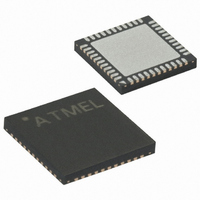
ATMEGA8515-16MU Atmel, ATMEGA8515-16MU Datasheet - Page 29

ATMEGA8515-16MU
Manufacturer Part Number
ATMEGA8515-16MU
Description
IC AVR MCU 8K 16MHZ 5V 44-QFN
Manufacturer
Atmel
Series
AVR® ATmegar
Specifications of ATMEGA8515-16MU
Core Processor
AVR
Core Size
8-Bit
Speed
16MHz
Connectivity
EBI/EMI, SPI, UART/USART
Peripherals
Brown-out Detect/Reset, POR, PWM, WDT
Number Of I /o
35
Program Memory Size
8KB (4K x 16)
Program Memory Type
FLASH
Eeprom Size
512 x 8
Ram Size
512 x 8
Voltage - Supply (vcc/vdd)
4.5 V ~ 5.5 V
Oscillator Type
Internal
Operating Temperature
-40°C ~ 85°C
Package / Case
44-VQFN Exposed Pad
Processor Series
ATMEGA8x
Core
AVR8
Data Bus Width
8 bit
Data Ram Size
512 B
Interface Type
SPI, USART
Maximum Clock Frequency
16 MHz
Number Of Programmable I/os
35
Number Of Timers
2
Operating Supply Voltage
4.5 V to 5.5 V
Maximum Operating Temperature
+ 85 C
Mounting Style
SMD/SMT
3rd Party Development Tools
EWAVR, EWAVR-BL
Development Tools By Supplier
ATAVRDRAGON, ATSTK500, ATSTK600, ATAVRISP2, ATAVRONEKIT
Minimum Operating Temperature
- 40 C
For Use With
ATAVRISP2 - PROGRAMMER AVR IN SYSTEMATSTK500 - PROGRAMMER AVR STARTER KIT
Lead Free Status / RoHS Status
Lead free / RoHS Compliant
Data Converters
-
Lead Free Status / Rohs Status
Details
- Current page: 29 of 257
- Download datasheet (2Mb)
XMEM Register
Description
MCU Control Register –
MCUCR
Extended MCU Control
Register – EMCUCR
2512K–AVR–01/10
Figure 16. External Data Memory Cycles with SRWn1 = 1 and SRWn0 = 1
Note:
• Bit 7 – SRE: External SRAM/XMEM Enable
Writing SRE to one enables the External Memory Interface.The pin functions AD7:0,
A15:8, ALE, WR, and RD are activated as the alternate pin functions. The SRE bit over-
rides any pin direction settings in the respective Data Direction Registers. Writing SRE
to zero, disables the External Memory Interface and the normal pin and data direction
settings are used.
• Bit 6 – SRW10: Wait State Select Bit
For a detailed description, see common description for the SRWn bits below (EMCUCR
description).
• Bit 6..4 – SRL2, SRL1, SRL0: Wait State Sector Limit
It is possible to configure different wait states for different external memory addresses.
The External Memory address space can be divided in two sectors that have separate
wait state bits. The SRL2, SRL1, and SRL0 bits select the splitting of these sectors, see
Table 2 and Figure 11. By default, the SRL2, SRL1, and SRL0 bits are set to zero and
the entire External Memory address space is treated as one sector. When the entire
System Clock (CLK
Bit
Read/Write
Initial Value
Bit
Read/Write
Initial Value
DA7:0 (XMBK = 0)
DA7:0 (XMBK = 1)
1. SRWn1 = SRW11 (upper sector) or SRW01 (lower sector), SRWn0 = SRW10 (upper
DA7:0
A15:8
CPU
ALE
WR
RD
sector) or SRW00 (lower sector)
The ALE pulse in period T7 is only present if the next instruction accesses the RAM
(internal or external).
)
Prev. Addr.
Prev. Data
Prev. Data
Prev. Data
SRE
R/W
SM0
R/W
7
0
7
0
T1
SRW10
SRL2
R/W
R/W
6
0
6
0
Address
Address
Address
T2
SRL1
R/W
R/W
SE
XX
5
0
5
0
Address
T3
SRL0
SM1
R/W
R/W
Data
Data
Data
4
0
4
0
SRW01
ISC11
R/W
R/W
T4
3
0
3
0
SRW00
ISC10
R/W
R/W
2
0
2
0
ATmega8515(L)
T5
SRW11
ISC01
R/W
R/W
1
0
1
0
T6
ISC00
ISC2
R/W
R/W
0
0
0
0
(1)
T7
EMCUCR
MCUCR
29
Related parts for ATMEGA8515-16MU
Image
Part Number
Description
Manufacturer
Datasheet
Request
R

Part Number:
Description:
IC AVR MCU 2.4GHZ XCEIVER 64QFN
Manufacturer:
Atmel
Datasheet:

Part Number:
Description:
Manufacturer:
Atmel
Datasheet:

Part Number:
Description:
MCU ATMEGA644/AT86RF230 40-DIP
Manufacturer:
Atmel
Datasheet:

Part Number:
Description:
BUNDLE ATMEGA644P/AT86RF230 QFN
Manufacturer:
Atmel
Datasheet:

Part Number:
Description:
BUNDLE ATMEGA644P/AT86RF230 TQFP
Manufacturer:
Atmel
Datasheet:

Part Number:
Description:
MCU ATMEGA1281/AT86RF230 64-TQFP
Manufacturer:
Atmel
Datasheet:

Part Number:
Description:
MCU ATMEGA1280/AT86RF230 100TQFP
Manufacturer:
Atmel
Datasheet:

Part Number:
Description:
BUNDLE ATMEGA1280/AT86RF100-TQFP
Manufacturer:
Atmel
Datasheet:

Part Number:
Description:
BUNDLE ATMEGA2560V/AT86RF230-ZU
Manufacturer:
Atmel
Datasheet:

Part Number:
Description:
MCU ATMEGA2561/AT86RF230 64-TQFP
Manufacturer:
Atmel
Datasheet:

Part Number:
Description:
INTERVAL AND WIPE/WASH WIPER CONTROL IC WITH DELAY
Manufacturer:
ATMEL Corporation
Datasheet:

Part Number:
Description:
Low-Voltage Voice-Switched IC for Hands-Free Operation
Manufacturer:
ATMEL Corporation
Datasheet:

Part Number:
Description:
MONOLITHIC INTEGRATED FEATUREPHONE CIRCUIT
Manufacturer:
ATMEL Corporation
Datasheet:

Part Number:
Description:
AM-FM Receiver IC U4255BM-M
Manufacturer:
ATMEL Corporation
Datasheet:


