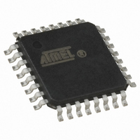
ATMEGA8U2-AU Atmel, ATMEGA8U2-AU Datasheet - Page 257

ATMEGA8U2-AU
Manufacturer Part Number
ATMEGA8U2-AU
Description
MCU AVR 8K FLASH 16MHZ 32TQFP
Manufacturer
Atmel
Series
AVR® ATmegar
Specifications of ATMEGA8U2-AU
Core Processor
AVR
Core Size
8-Bit
Speed
16MHz
Connectivity
SPI, UART/USART, USB
Peripherals
Brown-out Detect/Reset, POR, PWM, WDT
Number Of I /o
22
Program Memory Size
8KB (4K x 16)
Program Memory Type
FLASH
Eeprom Size
512 x 8
Ram Size
512 x 8
Voltage - Supply (vcc/vdd)
2.7 V ~ 5.5 V
Oscillator Type
Internal
Operating Temperature
-40°C ~ 85°C
Package / Case
32-TQFP, 32-VQFP
Processor Series
ATmega
Core
AVR
Data Bus Width
8 bit
Data Ram Size
512 B
Interface Type
SPI, USART, USB
Maximum Clock Frequency
16 MHz
Number Of Programmable I/os
22
Number Of Timers
2
Operating Supply Voltage
5 V
Maximum Operating Temperature
+ 85 C
Mounting Style
SMD/SMT
3rd Party Development Tools
EWAVR, EWAVR-BL
Development Tools By Supplier
ATAVRDRAGON, ATSTK500, ATSTK600, ATAVRISP2, ATAVRONEKIT, AT90USBKEY, ATEVK525
Minimum Operating Temperature
- 40 C
Operating Temperature Range
- 40 C to + 85 C
Lead Free Status / RoHS Status
Lead free / RoHS Compliant
Data Converters
-
Lead Free Status / Rohs Status
Details
Available stocks
Company
Part Number
Manufacturer
Quantity
Price
Company:
Part Number:
ATMEGA8U2-AU
Manufacturer:
Atmel
Quantity:
2 772
Part Number:
ATMEGA8U2-AU
Manufacturer:
ATMEL/爱特梅尔
Quantity:
20 000
- Current page: 257 of 309
- Download datasheet (6Mb)
25.7.9
25.7.10
25.7.11
7799D–AVR–11/10
Programming the Fuse High Bits
Programming the Extended Fuse Bits
Programming the Lock Bits
The algorithm for programming the Fuse High bits is as follows (refer to
Flash” on page 253
The algorithm for programming the Extended Fuse bits is as follows (refer to
Flash” on page 253
Figure 25-5. Programming the FUSES Waveforms
The algorithm for programming the Lock bits is as follows (refer to
page 253
The Lock bits can only be cleared by executing Chip Erase.
1. A: Load Command “0100 0000”.
2. C: Load Data Low Byte. Bit n = “0” programs and bit n = “1” erases the Fuse bit.
3. Set BS2, BS1 to “01”. This selects high data byte.
4. Give WR a negative pulse and wait for RDY/BSY to go high.
5. Set BS2, BS1 to “00”. This selects low data byte.
1. 1. A: Load Command “0100 0000”.
2. 2. C: Load Data Low Byte. Bit n = “0” programs and bit n = “1” erases the Fuse bit.
3. 3. Set BS2, BS1 to “10”. This selects extended data byte.
4. 4. Give WR a negative pulse and wait for RDY/BSY to go high.
5. 5. Set BS2, BS1 to “00”. This selects low data byte.
1. A: Load Command “0010 0000”.
2. C: Load Data Low Byte. Bit n = “0” programs the Lock bit. If LB mode 3 is programmed
3. Give WR a negative pulse and wait for RDY/BSY to go high.
RESET +12V
(LB1 and LB2 is programmed), it is not possible to program the Boot Lock bits by any
External Programming mode.
RDY/BSY
PAGEL
XTAL1
DATA
for details on Command and Data loading):
XA1
XA0
BS1
BS2
WR
OE
0x40
A
for details on Command and Data loading):
for details on Command and Data loading):
DATA
C
Write Fuse Low byte
XX
0x40
A
DATA
C
ATmega8U2/16U2/32U2
Write Fuse high byte
XX
“Programming the Flash” on
0x40
A
DATA
C
Write Extended Fuse byte
“Programming the
“Programming the
XX
257
Related parts for ATMEGA8U2-AU
Image
Part Number
Description
Manufacturer
Datasheet
Request
R

Part Number:
Description:
IC AVR MCU 8K 16MHZ 5V 32TQFP
Manufacturer:
Atmel
Datasheet:

Part Number:
Description:
IC AVR MCU 8K 16MHZ 5V 32-QFN
Manufacturer:
Atmel
Datasheet:

Part Number:
Description:
IC AVR MCU 8K 16MHZ 5V 28DIP
Manufacturer:
Atmel
Datasheet:

Part Number:
Description:
IC AVR MCU 8K 16MHZ COM 32-TQFP
Manufacturer:
Atmel
Datasheet:

Part Number:
Description:
IC AVR MCU 8K 16MHZ IND 32-TQFP
Manufacturer:
Atmel
Datasheet:

Part Number:
Description:
IC AVR MCU 8K 16MHZ COM 28-DIP
Manufacturer:
Atmel
Datasheet:

Part Number:
Description:
IC AVR MCU 8K 16MHZ IND 28-DIP
Manufacturer:
Atmel
Datasheet:

Part Number:
Description:
IC AVR MCU 8K 16MHZ COM 32-QFN
Manufacturer:
Atmel
Datasheet:

Part Number:
Description:
MCU AVR 8KB FLASH 16MHZ 32QFN
Manufacturer:
Atmel
Datasheet:

Part Number:
Description:
IC AVR MCU 8K 16MHZ IND 32-QFN
Manufacturer:
Atmel
Datasheet:

Part Number:
Description:
IC MCU AVR 8K 5V 16MHZ 32-TQFP
Manufacturer:
Atmel
Datasheet:

Part Number:
Description:
IC MCU AVR 8K 5V 16MHZ 32-QFN
Manufacturer:
Atmel
Datasheet:

Part Number:
Description:
IC MCU AVR 8K 5V 16MHZ 28-DIP
Manufacturer:
Atmel
Datasheet:


