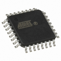
ATMEGA8A-AU Atmel, ATMEGA8A-AU Datasheet - Page 59

ATMEGA8A-AU
Manufacturer Part Number
ATMEGA8A-AU
Description
MCU AVR 8K FLASH 16MHZ 32-TQFP
Manufacturer
Atmel
Series
AVR® ATmegar
Specifications of ATMEGA8A-AU
Core Processor
AVR
Core Size
8-Bit
Speed
16MHz
Connectivity
I²C, SPI, UART/USART
Peripherals
Brown-out Detect/Reset, POR, PWM, WDT
Number Of I /o
23
Program Memory Size
8KB (4K x 16)
Program Memory Type
FLASH
Eeprom Size
512 x 8
Ram Size
1K x 8
Voltage - Supply (vcc/vdd)
2.7 V ~ 5.5 V
Data Converters
A/D 8x10b
Oscillator Type
Internal
Operating Temperature
-40°C ~ 85°C
Package / Case
32-TQFP, 32-VQFP
Processor Series
ATMEGA8x
Core
AVR8
Data Bus Width
8 bit
Data Ram Size
1 KB
Interface Type
SPI, TWI, USART
Maximum Clock Frequency
16 MHz
Number Of Programmable I/os
23
Number Of Timers
3
Maximum Operating Temperature
+ 85 C
Mounting Style
SMD/SMT
3rd Party Development Tools
EWAVR, EWAVR-BL
Development Tools By Supplier
ATAVRDRAGON, ATSTK500, ATSTK600, ATAVRISP2, ATAVRONEKIT
Minimum Operating Temperature
- 40 C
On-chip Adc
10 bit, 8 Channel
Controller Family/series
AVR MEGA
No. Of I/o's
23
Eeprom Memory Size
512Byte
Ram Memory Size
1KB
Cpu Speed
16MHz
Rohs Compliant
Yes
For Use With
ATSTK600 - DEV KIT FOR AVR/AVR32ATSTK500 - PROGRAMMER AVR STARTER KIT
Lead Free Status / RoHS Status
Lead free / RoHS Compliant
Available stocks
Company
Part Number
Manufacturer
Quantity
Price
Company:
Part Number:
ATMEGA8A-AU
Manufacturer:
NXP
Quantity:
1 001
Company:
Part Number:
ATMEGA8A-AU
Manufacturer:
ATM
Quantity:
10 000
Part Number:
ATMEGA8A-AU
Manufacturer:
ATMEL/爱特梅尔
Quantity:
20 000
ATmega8A
• MISO – Port B, Bit 4
MISO: Master Data input, Slave Data output pin for SPI channel. When the SPI is enabled as a
Master, this pin is configured as an input regardless of the setting of DDB4. When the SPI is
enabled as a Slave, the data direction of this pin is controlled by DDB4. When the pin is forced
by the SPI to be an input, the pull-up can still be controlled by the PORTB4 bit.
• MOSI/OC2 – Port B, Bit 3
MOSI: SPI Master Data output, Slave Data input for SPI channel. When the SPI is enabled as a
Slave, this pin is configured as an input regardless of the setting of DDB3. When the SPI is
enabled as a Master, the data direction of this pin is controlled by DDB3. When the pin is forced
by the SPI to be an input, the pull-up can still be controlled by the PORTB3 bit.
OC2, Output Compare Match Output: The PB3 pin can serve as an external output for the
Timer/Counter2 Compare Match. The PB3 pin has to be configured as an output (DDB3 set
(one)) to serve this function. The OC2 pin is also the output pin for the PWM mode timer
function.
• SS/OC1B – Port B, Bit 2
SS: Slave Select input. When the SPI is enabled as a Slave, this pin is configured as an input
regardless of the setting of DDB2. As a Slave, the SPI is activated when this pin is driven low.
When the SPI is enabled as a Master, the data direction of this pin is controlled by DDB2. When
the pin is forced by the SPI to be an input, the pull-up can still be controlled by the PORTB2 bit.
OC1B, Output Compare Match output: The PB2 pin can serve as an external output for the
Timer/Counter1 Compare Match B. The PB2 pin has to be configured as an output (DDB2 set
(one)) to serve this function. The OC1B pin is also the output pin for the PWM mode timer
function.
• OC1A – Port B, Bit 1
OC1A, Output Compare Match output: The PB1 pin can serve as an external output for the
Timer/Counter1 Compare Match A. The PB1 pin has to be configured as an output (DDB1 set
(one)) to serve this function. The OC1A pin is also the output pin for the PWM mode timer
function.
• ICP1 – Port B, Bit 0
ICP1 – Input Capture Pin: The PB0 pin can act as an Input Capture Pin for Timer/Counter1.
Table 12-3
and
Table 12-4
relate the alternate functions of Port B to the overriding signals
shown in
Figure 12-5 on page
56. SPI MSTR INPUT and SPI SLAVE OUTPUT constitute the
MISO signal, while MOSI is divided into SPI MSTR OUTPUT and SPI SLAVE INPUT.
59
8159D–AVR–02/11


