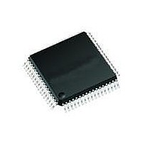
PIC16LF1947-I/PT Microchip Technology, PIC16LF1947-I/PT Datasheet - Page 123

PIC16LF1947-I/PT
Manufacturer Part Number
PIC16LF1947-I/PT
Description
IC MCU 8BIT FLASH 64TQFP
Manufacturer
Microchip Technology
Series
PIC® XLP™ 16Fr
Datasheets
1.PIC16LF1933-ISS.pdf
(46 pages)
2.PIC16LF1946-IPT.pdf
(448 pages)
3.PIC16LF1946-IPT.pdf
(6 pages)
Specifications of PIC16LF1947-I/PT
Program Memory Type
FLASH
Program Memory Size
28KB (16K x 14)
Package / Case
64-TFQFP
Core Processor
PIC
Core Size
8-Bit
Speed
32MHz
Connectivity
I²C, LIN, SPI, UART/USART
Peripherals
Brown-out Detect/Reset, LCD, POR, PWM, WDT
Number Of I /o
54
Eeprom Size
256 x 8
Ram Size
1K x 8
Voltage - Supply (vcc/vdd)
1.8 V ~ 3.6 V
Data Converters
A/D 17x10b
Oscillator Type
Internal
Operating Temperature
-40°C ~ 85°C
Processor Series
PIC16LF
Core
PIC
Data Bus Width
8 bit
Data Ram Size
1 KB
Interface Type
EUSART/I2C/SPI
Maximum Clock Frequency
32 MHz
Number Of Programmable I/os
54
Number Of Timers
5
Operating Supply Voltage
1.8 V to 3.6 V
Maximum Operating Temperature
+ 85 C
Mounting Style
SMD/SMT
3rd Party Development Tools
52715-96, 52716-328, 52717-734
Development Tools By Supplier
PG164130, DV164035, DV244005, DV164005
Minimum Operating Temperature
- 40 C
On-chip Adc
17-ch x 10-bit
A/d Bit Size
10 bit
A/d Channels Available
17
Height
1 mm
Length
10 mm
Supply Voltage (max)
5.5 V
Supply Voltage (min)
1.8 V
Width
10 mm
Lead Free Status / RoHS Status
Lead free / RoHS Compliant
Lead Free Status / RoHS Status
Lead free / RoHS Compliant, Lead free / RoHS Compliant
Available stocks
Company
Part Number
Manufacturer
Quantity
Price
Company:
Part Number:
PIC16LF1947-I/PT
Manufacturer:
FREESCALE
Quantity:
1 200
Company:
Part Number:
PIC16LF1947-I/PT
Manufacturer:
Microchip Technology
Quantity:
10 000
Part Number:
PIC16LF1947-I/PT
Manufacturer:
MICROCHIP/微芯
Quantity:
20 000
- Current page: 123 of 448
- Download datasheet (4Mb)
REGISTER 11-5:
2010 Microchip Technology Inc.
bit 7
Legend:
R = Readable bit
S = Bit can only be set
‘1’ = Bit is set
bit 7
bit 6
bit 5
bit 4
bit 3
bit 2
bit 1
bit 0
R/W-0/0
EEPGD
EEPGD: Flash Program/Data EEPROM Memory Select bit
1 = Accesses program space Flash memory
0 = Accesses data EEPROM memory
CFGS: Flash Program/Data EEPROM or Configuration Select bit
1 = Accesses Configuration, User ID and Device ID Registers
0 = Accesses Flash Program or data EEPROM Memory
LWLO: Load Write Latches Only bit
If CFGS = 1 (Configuration space) OR CFGS = 0 and EEPGD = 1 (program Flash):
If CFGS = 0 and EEPGD = 0: (Accessing data EEPROM)
LWLO is ignored. The next WR command initiates a write to the data EEPROM.
FREE: Program Flash Erase Enable bit
If CFGS = 1 (Configuration space) OR CFGS = 0 and EEPGD = 1 (program Flash):
If EEPGD = 0 and CFGS = 0: (Accessing data EEPROM)
FREE is ignored. The next WR command will initiate both a erase cycle and a write cycle.
WRERR: EEPROM Error Flag bit
1 = Condition indicates an improper program or erase sequence attempt or termination (bit is set
0 = The program or erase operation completed normally.
WREN: Program/Erase Enable bit
1 = Allows program/erase cycles
0 = Inhibits programming/erasing of program Flash and data EEPROM
WR: Write Control bit
1 = Initiates a program Flash or data EEPROM program/erase operation.
0 = Program/erase operation to the Flash or data EEPROM is complete and inactive.
RD: Read Control bit
1 = Initiates an program Flash or data EEPROM read. Read takes one cycle. RD is cleared in
0 = Does not initiate a program Flash or data EEPROM data read.
R/W-0/0
CFGS
1 = The next WR command does not initiate a write; only the program memory latches are
0 = The next WR command writes a value from EEDATH:EEDATL into program memory latches
1 = Performs an erase operation on the next WR command (cleared by hardware after
0 = Performs a write operation on the next WR command.
automatically on any set attempt (write ‘1’) of the WR bit).
The operation is self-timed and the bit is cleared by hardware once operation is complete.
The WR bit can only be set (not cleared) in software.
hardware. The RD bit can only be set (not cleared) in software.
EECON1: EEPROM CONTROL 1 REGISTER
updated.
and initiates a write of all the data stored in the program memory latches.
completion of erase).
W = Writable bit
x = Bit is unknown
‘0’ = Bit is cleared
R/W-0/0
LWLO
R/W/HC-0/0
FREE
Preliminary
U = Unimplemented bit, read as ‘0’
-n/n = Value at POR and BOR/Value at all other Resets
HC = Bit is cleared by hardware
WRERR
R/W-x/q
PIC16F/LF1946/47
R/W-0/0
WREN
R/S/HC-0/0
WR
DS41414B-page 123
R/S/HC-0/0
RD
bit 0
Related parts for PIC16LF1947-I/PT
Image
Part Number
Description
Manufacturer
Datasheet
Request
R

Part Number:
Description:
IC, 8BIT MCU, PIC16LF, 32MHZ, QFN-28
Manufacturer:
Microchip Technology
Datasheet:

Part Number:
Description:
IC, 8BIT MCU, PIC16LF, 32MHZ, QFN-28
Manufacturer:
Microchip Technology
Datasheet:

Part Number:
Description:
IC, 8BIT MCU, PIC16LF, 32MHZ, DIP-18
Manufacturer:
Microchip Technology
Datasheet:

Part Number:
Description:
IC, 8BIT MCU, PIC16LF, 20MHZ, TQFP-44
Manufacturer:
Microchip Technology
Datasheet:

Part Number:
Description:
7 KB Flash, 384 Bytes RAM, 32 MHz Int. Osc, 16 I/0, Enhanced Mid Range Core, Nan
Manufacturer:
Microchip Technology

Part Number:
Description:
14KB Flash, 512B RAM, LCD, 11x10b ADC, EUSART, NanoWatt XLP 28 SOIC .300in T/R
Manufacturer:
Microchip Technology
Datasheet:

Part Number:
Description:
14KB Flash, 512B RAM, LCD, 11x10b ADC, EUSART, NanoWatt XLP 28 SSOP .209in T/R
Manufacturer:
Microchip Technology
Datasheet:

Part Number:
Description:
MCU PIC 14KB FLASH XLP 28-SSOP
Manufacturer:
Microchip Technology

Part Number:
Description:
MCU PIC 14KB FLASH XLP 28-SOIC
Manufacturer:
Microchip Technology

Part Number:
Description:
MCU PIC 512B FLASH XLP 28-UQFN
Manufacturer:
Microchip Technology

Part Number:
Description:
MCU PIC 14KB FLASH XLP 28-SPDIP
Manufacturer:
Microchip Technology

Part Number:
Description:
MCU 7KB FLASH 256B RAM 40-UQFN
Manufacturer:
Microchip Technology

Part Number:
Description:
MCU 7KB FLASH 256B RAM 44-TQFP
Manufacturer:
Microchip Technology

Part Number:
Description:
MCU 14KB FLASH 1KB RAM 28-UQFN
Manufacturer:
Microchip Technology

Part Number:
Description:
MCU PIC 14KB FLASH XLP 40-UQFN
Manufacturer:
Microchip Technology


