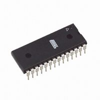
ATTINY28L-4PU Atmel, ATTINY28L-4PU Datasheet - Page 6

ATTINY28L-4PU
Manufacturer Part Number
ATTINY28L-4PU
Description
IC MCU 2K FLASH 4MHZ 28-DIP
Manufacturer
Atmel
Series
AVR® ATtinyr
Specifications of ATTINY28L-4PU
Core Processor
AVR
Core Size
8-Bit
Speed
4MHz
Peripherals
POR, WDT
Number Of I /o
11
Program Memory Size
2KB (1K x 16)
Program Memory Type
FLASH
Voltage - Supply (vcc/vdd)
2.7 V ~ 5.5 V
Oscillator Type
Internal
Operating Temperature
-40°C ~ 85°C
Package / Case
28-DIP (0.300", 7.62mm)
Processor Series
ATTINY2x
Core
AVR8
Data Bus Width
8 bit
Data Ram Size
32 B
Maximum Clock Frequency
4 MHz
Number Of Programmable I/os
11
Number Of Timers
1
Operating Supply Voltage
2.7 V to 5.5 V
Maximum Operating Temperature
+ 85 C
Mounting Style
Through Hole
3rd Party Development Tools
EWAVR, EWAVR-BL
Development Tools By Supplier
ATAVRDRAGON, ATSTK500, ATSTK600, ATAVRISP2, ATAVRONEKIT
Minimum Operating Temperature
- 40 C
On-chip Adc
8 bit
Package
28PDIP
Device Core
AVR
Family Name
ATtiny
Maximum Speed
4 MHz
Ram Size
32 Byte
For Use With
ATSTK600-DIP40 - STK600 SOCKET/ADAPTER 40-PDIPATSTK500 - PROGRAMMER AVR STARTER KIT
Lead Free Status / RoHS Status
Lead free / RoHS Compliant
Eeprom Size
-
Ram Size
-
Data Converters
-
Connectivity
-
Lead Free Status / Rohs Status
Details
Available stocks
Company
Part Number
Manufacturer
Quantity
Price
Part Number:
ATTINY28L-4PU
Manufacturer:
ATMEL/爱特梅尔
Quantity:
20 000
Status Register
Status Register – SREG
6
ATtiny28L/V
The AVR status register (SREG) at I/O space location $3F is defined as:
• Bit 7 – I: Global Interrupt Enable
The global interrupt enable bit must be set (one) for the interrupts to be enabled. The
individual interrupt enable control is then performed in separate control registers. If the
global interrupt enable register is cleared (zero), none of the interrupts are enabled inde-
pendent of the individual interrupt enable settings. The I-bit is cleared by hardware after
an interrupt has occurred, and is set by the RETI instruction to enable subsequent
interrupts.
• Bit 6 – T: Bit Copy Storage
The bit copy instructions BLD (Bit LoaD) and BST (Bit STore) use the T-bit as source
and destination for the operated bit. A bit from a register in the register file can be copied
into T by the BST instruction, and a bit in T can be copied into a bit in a register in the
register file by the BLD instruction.
• Bit 5 – H: Half-carry Flag
The half-carry flag H indicates a half-carry in some arithmetic operations. See the
Instruction Set description for detailed information.
• Bit 4 – S: Sign Bit, S = N ⊕ V
The S-bit is always an exclusive or between the negative flag N and the two’s comple-
ment overflow flag V. See the Instruction Set description for detailed information.
• Bit 3 – V: Two’s Complement Overflow Flag
The two’s complement overflow flag V supports two’s complement arithmetic. See the
Instruction Set description for detailed information.
• Bit 2 – N: Negative Flag
The negative flag N indicates a negative result from an arithmetical or logical operation.
See the Instruction Set description for detailed information.
• Bit 1 – Z: Zero Flag
The zero flag Z indicates a zero result from an arithmetical or logical operation. See the
Instruction Set description for detailed information.
• Bit 0 – C: Carry Flag
The carry flag C indicates a carry in an arithmetical or logical operation. See the Instruc-
tion Set description for detailed information.
Note that the status register is not automatically stored when entering an interrupt rou-
tine and restored when returning from an interrupt routine. This must be handled by
software.
Bit
$3F
Read/Write
Initial Value
R/W
7
0
I
R/W
6
T
0
R/W
H
5
0
R/W
S
4
0
R/W
V
3
0
R/W
2
N
0
R/W
1
Z
0
R/W
1062F–AVR–07/06
C
0
0
SREG


