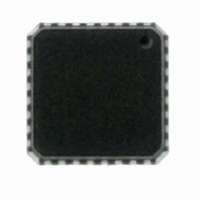
ATTINY26L-8MU Atmel, ATTINY26L-8MU Datasheet - Page 16

ATTINY26L-8MU
Manufacturer Part Number
ATTINY26L-8MU
Description
ID MCU AVR 2K 5V 8MHZ 32-QFN
Manufacturer
Atmel
Series
AVR® ATtinyr
Specifications of ATTINY26L-8MU
Core Processor
AVR
Core Size
8-Bit
Speed
8MHz
Connectivity
USI
Peripherals
Brown-out Detect/Reset, POR, PWM, WDT
Number Of I /o
16
Program Memory Size
2KB (1K x 16)
Program Memory Type
FLASH
Eeprom Size
128 x 8
Ram Size
128 x 8
Voltage - Supply (vcc/vdd)
2.7 V ~ 5.5 V
Data Converters
A/D 11x10b
Oscillator Type
Internal
Operating Temperature
-40°C ~ 85°C
Package / Case
32-VQFN Exposed Pad, 32-HVQFN, 32-SQFN, 32-DHVQFN
Processor Series
ATTINY2x
Core
AVR8
Data Bus Width
8 bit
Data Ram Size
128 B
Interface Type
2-Wire, ISP, SM-Bus, SPI, UART, USI
Maximum Clock Frequency
8 MHz
Number Of Programmable I/os
16
Number Of Timers
2
Operating Supply Voltage
2.7 V to 5.5 V
Maximum Operating Temperature
+ 85 C
Mounting Style
SMD/SMT
3rd Party Development Tools
EWAVR, EWAVR-BL
Development Tools By Supplier
ATAVRDRAGON, ATSTK500, ATSTK600, ATAVRISP2, ATAVRONEKIT
Minimum Operating Temperature
- 40 C
On-chip Adc
10 bit, 11 Channel
Cpu Family
ATtiny
Device Core
AVR
Device Core Size
8b
Frequency (max)
8MHz
Total Internal Ram Size
128Byte
# I/os (max)
16
Number Of Timers - General Purpose
2
Operating Supply Voltage (typ)
3.3/5V
Operating Supply Voltage (max)
5.5V
Operating Supply Voltage (min)
2.7V
Instruction Set Architecture
RISC
Operating Temp Range
-40C to 85C
Operating Temperature Classification
Industrial
Mounting
Surface Mount
Pin Count
32
Package Type
MLF EP
For Use With
ATSTK600 - DEV KIT FOR AVR/AVR32770-1007 - ISP 4PORT ATMEL AVR MCU SPI/JTAGATAVRISP2 - PROGRAMMER AVR IN SYSTEMATSTK505 - ADAPTER KIT FOR 14PIN AVR MCU
Lead Free Status / RoHS Status
Lead free / RoHS Compliant
Other names
ATTINY26L-8MJ
ATTINY26L-8MJ
ATTINY26L-8MJ
Available stocks
Company
Part Number
Manufacturer
Quantity
Price
Part Number:
ATTINY26L-8MU
Manufacturer:
ATMEL/爱特梅尔
Quantity:
20 000
Memories
The AVR CPU is driven by the System Clock Ø, directly generated from the external clock crys-
tal for the chip. No internal clock division is used.
Figure 16 shows the parallel instruction fetches and instruction executions enabled by the Har-
vard architecture and the fast-access Register File concept. This is the basic pipelining concept
to obtain up to 1 MIPS per MHz with the corresponding unique results for functions per cost,
functions per clocks, and functions per power-unit.
Figure 16. The Parallel Instruction Fetches and Instruction Executions
T1
T2
T3
T4
System Clock Ø
1st Instruction Fetch
1st Instruction Execute
2nd Instruction Fetch
2nd Instruction Execute
3rd Instruction Fetch
3rd Instruction Execute
4th Instruction Fetch
Figure 17 shows the internal timing concept for the Register File. In a single clock cycle an ALU
operation using two register operands is executed, and the result is stored back to the destina-
tion register.
Figure 17. Single Cycle ALU Operation
T1
T2
T3
T4
System Clock Ø
Total Execution Time
Register Operands Fetch
ALU Operation Execute
Result Write Back
The internal data SRAM access is performed in two System Clock cycles as described in Figure
18.
ATtiny26(L)
16
1477K–AVR–08/10


