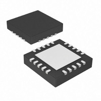
PIC18LF13K22-I/ML Microchip Technology, PIC18LF13K22-I/ML Datasheet - Page 22

PIC18LF13K22-I/ML
Manufacturer Part Number
PIC18LF13K22-I/ML
Description
IC PIC MCU FLASH 256KX8 20-QFN
Manufacturer
Microchip Technology
Series
PIC® XLP™ 18Fr
Datasheets
1.PIC18LF13K22-ISS.pdf
(388 pages)
2.PIC18LF13K22-ISS.pdf
(12 pages)
3.PIC18LF13K22-ISS.pdf
(36 pages)
4.PIC18LF14K22-IP.pdf
(382 pages)
Specifications of PIC18LF13K22-I/ML
Program Memory Type
FLASH
Program Memory Size
8KB (4K x 16)
Package / Case
20-VQFN Exposed Pad, 20-HVQFN, 20-SQFN, 20-DHVQFN
Core Processor
PIC
Core Size
8-Bit
Speed
64MHz
Connectivity
I²C, LIN, SPI, UART/USART
Peripherals
Brown-out Detect/Reset, POR, PWM, WDT
Number Of I /o
17
Eeprom Size
256 x 8
Ram Size
256 x 8
Voltage - Supply (vcc/vdd)
1.8 V ~ 3.6 V
Data Converters
A/D 12x10b
Oscillator Type
Internal
Operating Temperature
-40°C ~ 85°C
Processor Series
PIC18LF
Core
PIC
Data Bus Width
8 bit
Data Ram Size
256 B
Interface Type
I2C, MSSP, SPI, USART
Maximum Clock Frequency
32 KHz
Number Of Programmable I/os
18
Number Of Timers
4
Operating Supply Voltage
1.8 V to 3.6 V
Maximum Operating Temperature
+ 125 C
Mounting Style
SMD/SMT
3rd Party Development Tools
52715-96, 52716-328, 52717-734, 52712-325, EWPIC18
Development Tools By Supplier
PG164130, DV164035, DV244005, DV164005
Minimum Operating Temperature
- 40 C
On-chip Adc
10 bit, 12 Channel
Lead Free Status / RoHS Status
Lead free / RoHS Compliant
Lead Free Status / RoHS Status
Lead free / RoHS Compliant, Lead free / RoHS Compliant
Available stocks
Company
Part Number
Manufacturer
Quantity
Price
Company:
Part Number:
PIC18LF13K22-I/ML
Manufacturer:
CAVIUM
Quantity:
155
PIC18F1XK22/LF1XK22
5.0
5.1
Program Flash is accessed one byte at a time via the
4-bit command, ‘1001’ (table read, post-increment).
The contents of memory pointed to by the Table Pointer
(TBLPTRU:TBLPTRH:TBLPTRL) are serially output on
PGD.
TABLE 5-1:
FIGURE 5-1:
DS41357B-page 22
Step 1: Set Table Pointer
0000
0000
0000
0000
0000
0000
Step 2: Read memory and then shift out on PGD, LSb to MSb
1001
PGC
Command
PGD
Note 1:
4-bit
READING THE DEVICE
Read Program Flash, ID Locations
and Configuration Bits
Magnification of the high-impedance delay between PGC and PGD is shown in Figure 5-5.
1
1
READ PROGRAM FLASH SEQUENCE
2
0
0E <Addr[21:16]>
0E <Addr[15:8]>
0E <Addr[7:0]>
Data Payload
3
TABLE READ POST-INCREMENT INSTRUCTION TIMING DIAGRAM (1001)
0
4
6E F8
6E F7
6E F6
00 00
1
P5
PGD = Input
1
2
3
MOVLW Addr[21:16]
MOVWF TBLPTRU
MOVLW <Addr[15:8]>
MOVWF TBLPTRH
MOVLW <Addr[7:0]>
MOVWF TBLPTRL
TBLRD *+
4
Advance Information
5
6
7
8
P6
The 4-bit command is shifted in LSb first. The read is
executed during the next 8 clocks, then shifted out on
PGD during the last 8 clocks, LSb to MSb. A delay of
P6 must be introduced after the falling edge of the 8th
PGC of the operand to allow PGD to transition from an
input to an output. During this time, PGC must be held
low (see Figure 5-1). This operation also increments
the Table Pointer by one, pointing to the next byte in
program Flash for the next read.
This technique will work to read any memory in the
000000h to 3FFFFFh address space, so it also applies
to the reading of the ID and Configuration registers.
9
LSb
P14
10
1
Core Instruction
11
2
PGD = Output
12
Shift Data Out
3
13
4
14
5
15
© 2009 Microchip Technology Inc.
6
16
MSb
P5A
(Note 1)
Fetch Next 4-bit Command
1
PGD = Input
n
2
n
3
n
4
n


