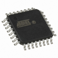
ATMEGA16U2-AU Atmel, ATMEGA16U2-AU Datasheet - Page 259

ATMEGA16U2-AU
Manufacturer Part Number
ATMEGA16U2-AU
Description
MCU AVR 16K FLASH USB 32TQFP
Manufacturer
Atmel
Series
AVR® ATmegar
Specifications of ATMEGA16U2-AU
Core Processor
AVR
Core Size
8-Bit
Speed
16MHz
Connectivity
SPI, UART/USART, USB
Peripherals
Brown-out Detect/Reset, POR, PWM, WDT
Number Of I /o
22
Program Memory Size
16KB (8K x 16)
Program Memory Type
FLASH
Eeprom Size
512 x 8
Ram Size
512 x 8
Voltage - Supply (vcc/vdd)
2.7 V ~ 5.5 V
Oscillator Type
Internal
Operating Temperature
-40°C ~ 85°C
Package / Case
32-TQFP, 32-VQFP
Processor Series
ATMEGA16x
Core
AVR8
Data Bus Width
8 bit
Data Ram Size
1.25 KB
Interface Type
SPI, UART
Maximum Clock Frequency
16 MHz
Number Of Programmable I/os
22
Number Of Timers
2
Maximum Operating Temperature
+ 85 C
Mounting Style
SMD/SMT
3rd Party Development Tools
EWAVR, EWAVR-BL
Development Tools By Supplier
ATAVRDRAGON, ATSTK500, ATSTK600, ATAVRISP2, ATAVRONEKIT, AT90USBKEY, ATEVK525
Minimum Operating Temperature
- 40 C
For Use With
ATSTK600 - DEV KIT FOR AVR/AVR32ATSTK500 - PROGRAMMER AVR STARTER KIT
Lead Free Status / RoHS Status
Lead free / RoHS Compliant
Data Converters
-
Lead Free Status / Rohs Status
Details
Available stocks
Company
Part Number
Manufacturer
Quantity
Price
- Current page: 259 of 309
- Download datasheet (6Mb)
25.8
25.9
7799D–AVR–11/10
Serial Downloading
Serial Programming Pin Mapping
Both the Flash and EEPROM memory arrays can be programmed using a serial programming
bus while RESET is pulled to GND. The serial programming interface consists of pins SCK, PDI
(input) and PDO (output). After RESET is set low, the Programming Enable instruction needs to
be executed first before program/erase operations can be executed. NOTE, in
page
dedicated for the internal Serial Peripheral Interface - SPI.
Table 25-14. Pin Mapping Serial Programming
Figure 25-7. Serial Programming and Verify
Notes:
When programming the EEPROM, an auto-erase cycle is built into the self-timed programming
operation (in the Serial mode ONLY) and there is no need to first execute the Chip Erase
instruction. The Chip Erase operation turns the content of every memory location in both the
Program and EEPROM arrays into 0xFF.
Depending on CKSEL Fuses, a valid clock must be present. The minimum low and high periods
for the serial clock (SCK) input are defined as follows:
Low: > 2 CPU clock cycles for f
High: > 2 CPU clock cycles for f
259, the pin mapping for serial programming is listed. Not all packages use the SPI pins
1. If the device is clocked by the internal Oscillator, it is no need to connect a clock source to the
2. V
Symbol
PDO
SCK
PDI
XTAL1 pin.
CC
- 0.3V < AVCC < V
PDO
SCK
PDI
ck
ck
CC
< 12 MHz, 3 CPU clock cycles for f
< 12 MHz, 3 CPU clock cycles for f
Pins
PB2
PB3
PB1
+ 0.3V, however, AVCC should always be within 1.8 - 5.5V
XTAL1
RESET
GND
(1)
ATmega8U2/16U2/32U2
AVCC
VCC
I/O
O
I
I
+1.8 - 5.5V
+1.8 - 5.5V
(2)
ck
ck
>= 12 MHz
>= 12 MHz
Serial Data out
Serial Data in
Description
Serial Clock
Table 25-14 on
259
Related parts for ATMEGA16U2-AU
Image
Part Number
Description
Manufacturer
Datasheet
Request
R

Part Number:
Description:
Manufacturer:
Atmel Corporation
Datasheet:

Part Number:
Description:
IC AVR MCU 16K 16MHZ 5V 44TQFP
Manufacturer:
Atmel
Datasheet:

Part Number:
Description:
IC AVR MCU 16K 16MHZ 5V 44-QFN
Manufacturer:
Atmel
Datasheet:

Part Number:
Description:
IC AVR MCU 16K 16MHZ 5V 40DIP
Manufacturer:
Atmel
Datasheet:

Part Number:
Description:
MCU AVR 16K FLASH 16MHZ 44-QFN
Manufacturer:
Atmel
Datasheet:

Part Number:
Description:
IC AVR MCU 16K 16MHZ COM 40-DIP
Manufacturer:
Atmel
Datasheet:

Part Number:
Description:
IC AVR MCU 16K 16MHZ COM 44-QFN
Manufacturer:
Atmel
Datasheet:

Part Number:
Description:
IC AVR MCU 16K 16MHZ IND 40-DIP
Manufacturer:
Atmel
Datasheet:

Part Number:
Description:
IC AVR MCU 16K 16MHZ IND 44-QFN
Manufacturer:
Atmel
Datasheet:

Part Number:
Description:
IC AVR MCU 16K 16MHZ IND 44-TQFP
Manufacturer:
Atmel
Datasheet:

Part Number:
Description:
IC MCU 8BIT 16KB FLASH 44TQFP
Manufacturer:
Atmel
Datasheet:

Part Number:
Description:
MCU AVR 16K FLASH 16MHZ 44-TQFP
Manufacturer:
Atmel
Datasheet:

Part Number:
Description:
IC AVR MCU 16K 16MHZ COM 44-TQFP
Manufacturer:
Atmel
Datasheet:


