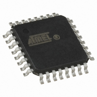
AT89LP828-20MH Atmel, AT89LP828-20MH Datasheet - Page 113

AT89LP828-20MH
Manufacturer Part Number
AT89LP828-20MH
Description
MCU 8051 8K FLASH SPI 32VQFN
Manufacturer
Atmel
Series
89LPr
Datasheet
1.AT89LP428-20AU.pdf
(149 pages)
Specifications of AT89LP828-20MH
Core Processor
8051
Core Size
8-Bit
Speed
20MHz
Connectivity
SPI, UART/USART
Peripherals
Brown-out Detect/Reset, POR, PWM, WDT
Number Of I /o
30
Program Memory Size
8KB (8K x 8)
Program Memory Type
FLASH
Eeprom Size
1K x 8
Ram Size
768 x 8
Voltage - Supply (vcc/vdd)
2.4 V ~ 5.5 V
Oscillator Type
Internal
Operating Temperature
-40°C ~ 85°C
Package / Case
32-TQFP
Lead Free Status / RoHS Status
Lead free / RoHS Compliant
Data Converters
-
Available stocks
Company
Part Number
Manufacturer
Quantity
Price
Company:
Part Number:
AT89LP828-20MH
Manufacturer:
Atmel
Quantity:
720
22. On-chip Debug System
22.1
3654A–MICRO–8/09
Physical Interface
The AT89LP428/828 On-chip Debug (OCD) System uses a 2-wire serial interface to control pro-
gram flow; read, modify, and write the system state; and program the nonvolatile memory. The
OCD System has the following features:
The On-chip Debug System uses a 2-wire synchronous serial interface to establish communica-
tion between the target device and the controlling emulator system. The OCD interface is
controlled by two User Fuses. OCD is enabled by clearing the OCD Enable Fuse. The OCD
device connections are shown in
ured as an input for the Debug Clock (DCL). Either the XTAL1, XTAL2 or P3.7 pin is configured
as a bi-directional data line for the Debug Data (DDA) depending on the clock source selected. If
the Internal RC Oscillator is selected, XTAL1 is configured as DDA (A). If the External Clock is
selected, XTAL2 is configured as DDA (B). If the Crystal Oscillator is selected, P3.7 is config-
ured as DDA (C). When OCD is enabled, the type of interface used depends on the OCD
Interface Select User Fuse. This fuse selects between a normal Two-wire Interface (TWI) and a
fast Two-wire Interface (FTWI). It is the duty of the user to program this fuse to the correct set-
ting for their debug system at the same time they enable OCD (see
on page
When designing a system where On-chip Debug will be used, the following observations must
be considered for correct operation:
• Complete program flow control
• Read-modify-write access to all internal SFRs and data memories
• Four hardware program address breakpoints
• Unlimited program software breakpoints using BREAK instruction
• Break on change in program memory flow
• Break on stack overflow/underflow
• Break on Watchdog overflow
• Break on reset
• Non-intrusive operation
• Programming of nonvolatile memory
• P3.6/RST cannot be connected directly to V
• All external reset sources must be removed.
• If P3.7 needs to be debugged in-system using the crystal oscillator, the external clock option
must be removed.
should be selected. The quartz crystal and any capacitors on XTAL1 or XTAL2 must be
removed and an external clock signal must be driven on XTAL1. Some emulator systems may
provide a user-configurable clock for this purpose.
121).
Figure
22-1. When OCD is enabled, the RST port pin is config-
CC
and any external capacitors connected to RST
AT89LP428/828
“User Configuration Fuses”
113


