ATMEGA48PV-10MMUR Atmel, ATMEGA48PV-10MMUR Datasheet - Page 304
ATMEGA48PV-10MMUR
Manufacturer Part Number
ATMEGA48PV-10MMUR
Description
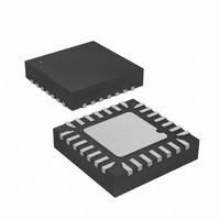
MCU AVR 4K FLASH 10MHZ 28QFN
Manufacturer
Atmel
Series
AVR® ATmegar
Datasheet
1.ATMEGA168P-20AU.pdf
(420 pages)
Specifications of ATMEGA48PV-10MMUR
Core Processor
AVR
Core Size
8-Bit
Speed
10MHz
Connectivity
I²C, SPI, UART/USART
Peripherals
Brown-out Detect/Reset, POR, PWM, WDT
Number Of I /o
23
Program Memory Size
4KB (2K x 16)
Program Memory Type
FLASH
Eeprom Size
256 x 8
Ram Size
512 x 8
Voltage - Supply (vcc/vdd)
1.8 V ~ 5.5 V
Data Converters
A/D 8x10b
Oscillator Type
Internal
Operating Temperature
-40°C ~ 85°C
Package / Case
*
Lead Free Status / RoHS Status
Lead free / RoHS Compliant


27.7.14
27.7.15
27.8
8025L–AVR–7/10
Serial Downloading
Reading the Calibration Byte
Parallel Programming Characteristics
The algorithm for reading the Calibration byte is as follows (refer to
page 298
1. A: Load Command “0000 1000”.
2. B: Load Address Low Byte, 0x00.
3. Set OE to “0”, and BS1 to “1”. The Calibration byte can now be read at DATA.
4. Set OE to “1”.
For chracteristics of the Parallel Programming, see
page
Both the Flash and EEPROM memory arrays can be programmed using the serial SPI bus while
RESET is pulled to GND. The serial interface consists of pins SCK, MOSI (input) and MISO (out-
put). After RESET is set low, the Programming Enable instruction needs to be executed first
before program/erase operations can be executed. NOTE, in
mapping for SPI programming is listed. Not all parts use the SPI pins dedicated for the internal
SPI interface.
Figure 27-7. Serial Programming and Verify
Notes:
When programming the EEPROM, an auto-erase cycle is built into the self-timed programming
operation (in the Serial mode ONLY) and there is no need to first execute the Chip Erase
instruction. The Chip Erase operation turns the content of every memory location in both the
Program and EEPROM arrays into 0xFF.
Depending on CKSEL Fuses, a valid clock must be present. The minimum low and high periods
for the serial clock (SCK) input are defined as follows:
Low: > 2 CPU clock cycles for f
High: > 2 CPU clock cycles for f
320.
1. If the device is clocked by the internal Oscillator, it is no need to connect a clock source to the
2. V
for details on Command and Address loading):
XTAL1 pin.
CC
- 0.3V <
AV
CC
< V
MOSI
MISO
SCK
ck
ck
CC
< 12 MHz, 3 CPU clock cycles for f
< 12 MHz, 3 CPU clock cycles for f
+ 0.3V, however,
XTAL1
RESET
GND
(1)
AV
”Parallel Programming Characteristics” on
CC
AVCC
ATmega48P/88P/168P
VCC
should always be within 1.8 - 5.5V
+1.8 - 5.5V
+1.8 - 5.5V
Table 27-15 on page
(2)
”Programming the Flash” on
ck
ck
>= 12 MHz
>= 12 MHz
305, the pin
304
Related parts for ATMEGA48PV-10MMUR
Image
Part Number
Description
Manufacturer
Datasheet
Request
R

Part Number:
Description:
MCU AVR 4K ISP FLASH 10MHZ 32QFN
Manufacturer:
Atmel
Datasheet:

Part Number:
Description:
MCU AVR 4K ISP FLASH 10MHZ 28DIP
Manufacturer:
Atmel
Datasheet:

Part Number:
Description:
MCU AVR 4K ISP FLSH 10MHZ 32TQFP
Manufacturer:
Atmel
Datasheet:
Part Number:
Description:
MCU AVR 4K FLASH 10MHZ 32TQFP
Manufacturer:
Atmel
Datasheet:

Part Number:
Description:
MCU AVR 4K FLASH 10MHZ 32QFN
Manufacturer:
Atmel
Datasheet:

Part Number:
Description:
MCU AVR 4K FLASH 10MHZ 28-QFN
Manufacturer:
Atmel
Datasheet:

Part Number:
Description:
Manufacturer:
Atmel Corporation
Datasheet:

Part Number:
Description:
MCU AVR 4K ISP FLASH 20MHZ 32QFN
Manufacturer:
Atmel
Datasheet:
Part Number:
Description:
MCU AVR 4K ISP FLSH 20MHZ 32TQFP
Manufacturer:
Atmel
Datasheet:
Part Number:
Description:
MCU AVR 4K ISP FLASH 20MHZ 28DIP
Manufacturer:
Atmel
Datasheet:
Part Number:
Description:
MCU AVR 4K FLASH 20MHZ 32TQFP
Manufacturer:
Atmel
Datasheet: