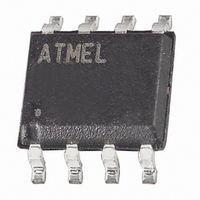
ATTINY13-20SU Atmel, ATTINY13-20SU Datasheet - Page 94

ATTINY13-20SU
Manufacturer Part Number
ATTINY13-20SU
Description
IC MCU AVR 1K FLASH 20MHZ 8SOIC
Manufacturer
Atmel
Series
AVR® ATtinyr
Specifications of ATTINY13-20SU
Core Processor
AVR
Core Size
8-Bit
Speed
20MHz
Peripherals
Brown-out Detect/Reset, POR, PWM, WDT
Number Of I /o
6
Program Memory Size
1KB (512 x 16)
Program Memory Type
FLASH
Eeprom Size
64 x 8
Ram Size
64 x 8
Voltage - Supply (vcc/vdd)
2.7 V ~ 5.5 V
Data Converters
A/D 4x10b
Oscillator Type
Internal
Operating Temperature
-40°C ~ 85°C
Package / Case
8-SOIC (5.3mm Width), 8-SOP, 8-SOEIAJ
Package
8SOIC EIAJ
Device Core
AVR
Family Name
ATtiny
Maximum Speed
20 MHz
Operating Supply Voltage
3.3|5 V
Data Bus Width
8 Bit
Number Of Programmable I/os
6
Interface Type
SPI
On-chip Adc
4-chx10-bit
Number Of Timers
1
For Use With
ATSTK600-DIP40 - STK600 SOCKET/ADAPTER 40-PDIP770-1007 - ISP 4PORT ATMEL AVR MCU SPI/JTAG770-1004 - ISP 4PORT FOR ATMEL AVR MCU SPIATAVRDRAGON - KIT DRAGON 32KB FLASH MEM AVRATAVRISP2 - PROGRAMMER AVR IN SYSTEMATJTAGICE2 - AVR ON-CHIP D-BUG SYSTEM
Lead Free Status / RoHS Status
Lead free / RoHS Compliant
Connectivity
-
- Current page: 94 of 176
- Download datasheet (3Mb)
14.12.4
14.12.5
94
ATtiny13
ADCSRB – ADC Control and Status Register B
DIDR0 – Digital Input Disable Register 0
The ADLAR bit in ADMUX, and the MUXn bits in ADMUX affect the way the result is read from
the registers. If ADLAR is set, the result is left adjusted. If ADLAR is cleared (default), the result
is right adjusted.
• ADC9:0: ADC Conversion Result
These bits represent the result from the conversion, as detailed in
page
• Bits 7, 5:3 – Res: Reserved Bits
These bits are reserved bits in the ATtiny13 and will always read as zero.
• Bits 2:0 – ADTS2:0: ADC Auto Trigger Source
If ADATE in ADCSRA is written to one, the value of these bits selects which source will trigger
an ADC conversion. If ADATE is cleared, the ADTS2:0 settings will have no effect. A conversion
will be triggered by the rising edge of the selected Interrupt Flag. Note that switching from a trig-
ger source that is cleared to a trigger source that is set, will generate a positive edge on the
trigger signal. If ADEN in ADCSRA is set, this will start a conversion. Switching to Free Running
mode (ADTS[2:0]=0) will not cause a trigger event, even if the ADC Interrupt Flag is set
Table 14-5.
• Bits 5:2 – ADC3D:ADC0D: ADC3:0 Digital Input Disable
When a bit is written logic one, the digital input buffer on the corresponding ADC pin is disabled.
The corresponding PIN register bit will always read as zero when this bit is set. When an analog
signal is applied to the ADC7..0 pin and the digital input from this pin is not needed, this bit
should be written logic one to reduce power consumption in the digital input buffer.
Bit
Read/Write
Initial Value
Bit
Read/Write
Initial Value
91.
ADTS2
0
0
0
0
1
1
1
ADC Auto Trigger Source Selections
R
R
7
–
0
7
–
0
ACME
ADTS1
R/W
R
6
–
0
6
0
0
0
1
1
0
0
1
ADC0D
R/W
5
0
R
5
–
0
ADC2D
R/W
ADTS0
R
4
0
4
–
0
0
1
0
1
0
1
0
ADC3D
R/W
R
3
0
3
–
0
Trigger Source
Free Running mode
Analog Comparator
External Interrupt Request 0
Timer/Counter Compare Match A
Timer/Counter Overflow
Timer/Counter Compare Match B
Pin Change Interrupt Request
ADC1D
ADTS2
R/W
R/W
2
0
2
0
“ADC Conversion Result” on
ADTS1
AIN1D
R/W
R/W
1
0
1
0
ADTS0
AIN0D
R/W
R/W
0
0
0
0
2535J–AVR–08/10
ADCSRB
.
DIDR0
Related parts for ATTINY13-20SU
Image
Part Number
Description
Manufacturer
Datasheet
Request
R

Part Number:
Description:
IC MCU AVR 1K FLASH 20MHZ 8SOIC
Manufacturer:
Atmel
Datasheet:

Part Number:
Description:
Manufacturer:
Atmel Corporation
Datasheet:

Part Number:
Description:
IC MCU AVR 1K FLASH 20MHZ 8SOIC
Manufacturer:
Atmel
Datasheet:

Part Number:
Description:
IC MCU AVR 1K FLASH 10MHZ 20-MLF
Manufacturer:
Atmel
Datasheet:

Part Number:
Description:
IC MCU AVR 1K FLASH 20MHZ 8DIP
Manufacturer:
Atmel
Datasheet:

Part Number:
Description:
MCU AVR 1KB FLASH 20MHZ 3X3 QFN
Manufacturer:
Atmel
Datasheet:

Part Number:
Description:
IC MCU AVR 1K 5V 20MHZ 8DIP
Manufacturer:
Atmel
Datasheet:

Part Number:
Description:
IC MCU AVR 1K 5V 20MHZ 8SOIC
Manufacturer:
Atmel
Datasheet:

Part Number:
Description:
IC MCU AVR 1K 5V 20MHZ 8SOIC
Manufacturer:
Atmel
Datasheet:

Part Number:
Description:
IC MCU AVR 1K FLASH 20MHZ 8DIP
Manufacturer:
Atmel
Datasheet:

Part Number:
Description:
IC MCU AVR 1K FLASH 20MHZ 8SOIC
Manufacturer:
Atmel
Datasheet:

Part Number:
Description:
MCU AVR 1KB FLASH 20MHZ 8SOIC GW
Manufacturer:
Atmel
Datasheet:


