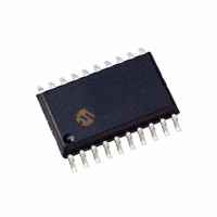
PIC16F631-I/SO Microchip Technology, PIC16F631-I/SO Datasheet - Page 109

PIC16F631-I/SO
Manufacturer Part Number
PIC16F631-I/SO
Description
IC PIC MCU FLASH 1KX14 20SOIC
Manufacturer
Microchip Technology
Series
PIC® 16Fr
Datasheets
1.PIC16F616T-ISL.pdf
(8 pages)
2.PIC16F690DM-PCTLHS.pdf
(306 pages)
3.PIC16F677-IP.pdf
(2 pages)
4.PIC16F677-IP.pdf
(16 pages)
5.PIC16F677-ISO.pdf
(294 pages)
Specifications of PIC16F631-I/SO
Program Memory Type
FLASH
Program Memory Size
1.75KB (1K x 14)
Package / Case
20-SOIC (7.5mm Width)
Core Processor
PIC
Core Size
8-Bit
Speed
20MHz
Peripherals
Brown-out Detect/Reset, POR, WDT
Number Of I /o
18
Eeprom Size
128 x 8
Ram Size
64 x 8
Voltage - Supply (vcc/vdd)
2 V ~ 5.5 V
Oscillator Type
Internal
Operating Temperature
-40°C ~ 85°C
Processor Series
PIC16F
Core
PIC
Data Bus Width
8 bit
Data Ram Size
64 B
Maximum Clock Frequency
20 MHz
Number Of Programmable I/os
17
Number Of Timers
2
Operating Supply Voltage
2 V to 5.5 V
Maximum Operating Temperature
+ 85 C
Mounting Style
SMD/SMT
3rd Party Development Tools
52715-96, 52716-328, 52717-734
Development Tools By Supplier
PG164130, DV164035, DV244005, DV164005, PG164120, ICE2000, DM163014, DM164120-4
Minimum Operating Temperature
- 40 C
Lead Free Status / RoHS Status
Lead free / RoHS Compliant
For Use With
658-1047-5 - BOARD EVALUATION ACCESSTOUCHAC162061 - HEADER INTRFC MPLAB ICD2 20PINAC164039 - MODULE SKT PROMATE II 20DIP/SOIC
Data Converters
-
Connectivity
-
Lead Free Status / Rohs Status
Lead free / RoHS Compliant
Available stocks
Company
Part Number
Manufacturer
Quantity
Price
Company:
Part Number:
PIC16F631-I/SO
Manufacturer:
ST
Quantity:
56
Part Number:
PIC16F631-I/SO
Manufacturer:
MICROCHIP/微芯
Quantity:
20 000
- PIC16F616T-ISL PDF datasheet
- PIC16F690DM-PCTLHS PDF datasheet #2
- PIC16F677-IP PDF datasheet #3
- PIC16F677-IP PDF datasheet #4
- PIC16F677-ISO PDF datasheet #5
- Current page: 109 of 306
- Download datasheet (6Mb)
9.0
The
conversion of an analog input signal to a 10-bit binary
representation of that signal. This device uses analog
inputs, which are multiplexed into a single sample and
hold circuit. The output of the sample and hold is
connected to the input of the converter. The converter
generates a 10-bit binary result via successive
approximation and stores the conversion result into the
ADC result registers (ADRESL and ADRESH).
The ADC voltage reference is software selectable to be
either internally generated or externally supplied.
The ADC can generate an interrupt upon completion of
a conversion. This interrupt can be used to wake-up the
device from Sleep.
FIGURE 9-1:
© 2008 Microchip Technology Inc.
Note:
Analog-to-Digital
ANALOG-TO-DIGITAL
CONVERTER (ADC) MODULE
RA0/AN0/C1IN+/ICSPDAT/ULPWU
Note 1:
RA1/AN1/C12IN0-/V
The ADC module applies to PIC16F677/
PIC16F685/PIC16F687/PIC16F689/
PIC16F690 devices only.
RA4/AN3/T1G/OSC2/CLKOUT
RA2/AN2/T0CKI/INT/C1OUT
2:
3:
RC2/AN6/C12IN2-/P1D
RC3/AN7/C12IN3-/P1C
RB4/AN10/SDI/SDA
P1C and P1D available on PIC16F685/PIC16F690 only.
SS, SDO, SDA, RX and DT available on PIC16F677/PIC16F687/PIC16F689/PIC16F690 only.
ADC module applies to the PIC16F677/PIC16F685/PIC16F687/PIC16F689/PIC16F690 devices only.
ADC BLOCK DIAGRAM
RB5/AN11/RX/DT
RC1/AN5/C12IN1-
RC7/AN9/SDO
Converter
RC0/AN4/C2IN+
RC6/AN8/SS
VP6 Reference
REF
/ICSPCLK
CV
PIC16F631/677/685/687/689/690
REF
(ADC)
(1)
(1)
(2)
(2)
(2)
(2)
CHS
allows
V
REF
V
GO/DONE
DD
Figure 9-1 shows the block diagram of the ADC.
VCFG = 0
VCFG = 1
ADON
V
SS
ADC
ADFM
ADRESH ADRESL
0 = Left Justify
1 = Right Justify
DS41262E-page 107
10
10
Related parts for PIC16F631-I/SO
Image
Part Number
Description
Manufacturer
Datasheet
Request
R

Part Number:
Description:
IC PIC MCU FLASH 1KX14 20SSOP
Manufacturer:
Microchip Technology
Datasheet:

Part Number:
Description:
IC PIC MCU FLASH 1KX14 20DIP
Manufacturer:
Microchip Technology
Datasheet:

Part Number:
Description:
IC PIC MCU FLASH 1KX14 20SOIC
Manufacturer:
Microchip Technology
Datasheet:

Part Number:
Description:
IC PIC MCU FLASH 1KX14 20DIP
Manufacturer:
Microchip Technology
Datasheet:

Part Number:
Description:
IC,MICROCONTROLLER,8-BIT,PIC CPU,CMOS,LLCC,20PIN,PLASTIC
Manufacturer:
Microchip Technology
Datasheet:

Part Number:
Description:
IC,MICROCONTROLLER,8-BIT,PIC CPU,CMOS,SSOP,20PIN,PLASTIC
Manufacturer:
Microchip Technology
Datasheet:

Part Number:
Description:
IC,MICROCONTROLLER,8-BIT,PIC CPU,CMOS,LLCC,20PIN,PLASTIC
Manufacturer:
Microchip Technology
Datasheet:

Part Number:
Description:
IC, 8BIT MCU, PIC16F, 32MHZ, SOIC-18
Manufacturer:
Microchip Technology
Datasheet:

Part Number:
Description:
IC, 8BIT MCU, PIC16F, 32MHZ, SSOP-20
Manufacturer:
Microchip Technology
Datasheet:

Part Number:
Description:
IC, 8BIT MCU, PIC16F, 32MHZ, DIP-18
Manufacturer:
Microchip Technology
Datasheet:

Part Number:
Description:
IC, 8BIT MCU, PIC16F, 32MHZ, QFN-28
Manufacturer:
Microchip Technology
Datasheet:

Part Number:
Description:
IC, 8BIT MCU, PIC16F, 32MHZ, QFN-28
Manufacturer:
Microchip Technology
Datasheet:

Part Number:
Description:
IC, 8BIT MCU, PIC16F, 32MHZ, QFN-28
Manufacturer:
Microchip Technology
Datasheet:

Part Number:
Description:
IC, 8BIT MCU, PIC16F, 32MHZ, SSOP-20
Manufacturer:
Microchip Technology
Datasheet:

Part Number:
Description:
IC, 8BIT MCU, PIC16F, 20MHZ, DIP-40
Manufacturer:
Microchip Technology
Datasheet:


