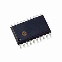
PIC16F690-E/SO Microchip Technology, PIC16F690-E/SO Datasheet - Page 79

PIC16F690-E/SO
Manufacturer Part Number
PIC16F690-E/SO
Description
IC PIC MCU FLASH 4KX14 20SOIC
Manufacturer
Microchip Technology
Series
PIC® 16Fr
Datasheets
1.PIC16F616T-ISL.pdf
(8 pages)
2.PIC16F690DM-PCTLHS.pdf
(306 pages)
3.PIC16F677-IP.pdf
(2 pages)
4.PIC16F677-IP.pdf
(16 pages)
5.PIC16F677-ISO.pdf
(294 pages)
Specifications of PIC16F690-E/SO
Program Memory Type
FLASH
Program Memory Size
7KB (4K x 14)
Package / Case
20-SOIC (7.5mm Width)
Core Processor
PIC
Core Size
8-Bit
Speed
20MHz
Connectivity
I²C, SPI, UART/USART
Peripherals
Brown-out Detect/Reset, POR, PWM, WDT
Number Of I /o
18
Eeprom Size
256 x 8
Ram Size
256 x 8
Voltage - Supply (vcc/vdd)
2 V ~ 5.5 V
Data Converters
A/D 12x10b
Oscillator Type
Internal
Operating Temperature
-40°C ~ 125°C
Processor Series
PIC16F
Core
PIC
Data Bus Width
8 bit
Data Ram Size
256 B
Interface Type
I2C/SPI/SSP/EUSART
Maximum Clock Frequency
20 MHz
Number Of Programmable I/os
17
Number Of Timers
3
Operating Supply Voltage
2 V to 5.5 V
Maximum Operating Temperature
+ 125 C
Mounting Style
SMD/SMT
3rd Party Development Tools
52715-96, 52716-328, 52717-734
Development Tools By Supplier
PG164130, DV164035, DV244005, DV164005, PG164120, ICE2000, DM163014, DM164120-1, DM163029
Minimum Operating Temperature
- 40 C
On-chip Adc
12-ch x 10-bit
Lead Free Status / RoHS Status
Lead free / RoHS Compliant
For Use With
XLT20SO1-1 - SOCKET TRANS ICE 20DIP TO 20SOICPIC16F690DM-PCTLHS - BOARD DEMO PICTAIL HUMIDITY SNSRAC162061 - HEADER INTRFC MPLAB ICD2 20PINAC164039 - MODULE SKT PROMATE II 20DIP/SOIC
Lead Free Status / Rohs Status
Lead free / RoHS Compliant
- PIC16F616T-ISL PDF datasheet
- PIC16F690DM-PCTLHS PDF datasheet #2
- PIC16F677-IP PDF datasheet #3
- PIC16F677-IP PDF datasheet #4
- PIC16F677-ISO PDF datasheet #5
- Current page: 79 of 294
- Download datasheet (6Mb)
4.5.1
The RC0 is configurable to function as one of the
following:
• a general purpose I/O
• an analog input for the ADC (except PIC16F631)
• an analog input to Comparator C2
4.5.2
The RC1 is configurable to function as one of the
following:
• a general purpose I/O
• an analog input for the ADC
• an analog input to Comparator C1 or C2
FIGURE 4-11:
© 2006 Microchip Technology Inc.
PORTC
PORTC
Data Bus
TRISC
TRISC
WR
WR
RD
RD
Note
1:
2:
D
D
To Comparators
To A/D Converter
CK
CK
RC0/AN4/C2IN+
RC1/AN5/C12IN1-
ANSEL determines Analog Input mode.
Not implemented on PIC16F631.
Q
Q
Q
Q
BLOCK DIAGRAM OF RC0
AND RC1
(2)
Analog Input
Mode
(1)
PIC16F631/677/685/687/689/690
V
V
DD
SS
I/O Pin
Preliminary
4.5.3
The RC2/AN6/P1D
one of the following:
• a general purpose I/O
• an analog input for the ADC (except PIC16F631)
• a PWM output
• an analog input to Comparator C1 or C2
4.5.4
The RC3/AN7/P1C
of the following:
• a general purpose I/O
• an analog input for the ADC (except PIC16F631)
• a PWM output
• a PWM output
• an analog input to Comparator C1 or C2
FIGURE 4-12:
PORTC
PORTC
TRISC
TRISC
Data Bus
Note 1: P1D is available on
Note 1: P1C is available on
WR
WR
RD
RD
Note
Available on PIC16F685/PIC16F690 only.
D
D
1:
2:
To Comparators
To A/D Converter
CK
CK
RC2/AN6/C12IN2-/P1D
RC3/AN7/C12IN3-/P1C
PIC16F685/PIC16F690 only.
PIC16F685/PIC16F690 only.
ANSEL determines Analog Input mode.
Not implemented on PIC16F631.
Q
Q
Q
Q
(1)
(1)
CCP1OUT
CCP1OUT
is configurable to function as one
BLOCK DIAGRAM OF RC2
AND RC3
Enable
is configurable to function as
(2)
Analog Input
Mode
1
0
0
1
(1)
DS41262C-page 77
V
V
DD
SS
I/O Pin
Related parts for PIC16F690-E/SO
Image
Part Number
Description
Manufacturer
Datasheet
Request
R

Part Number:
Description:
Manufacturer:
Microchip Technology Inc.
Datasheet:

Part Number:
Description:
IC PIC MCU FLASH 4KX14 20SSOP
Manufacturer:
Microchip Technology
Datasheet:

Part Number:
Description:
IC PIC MCU FLASH 4KX14 20DIP
Manufacturer:
Microchip Technology
Datasheet:

Part Number:
Description:
IC PIC MCU FLASH 4KX14 20SOIC
Manufacturer:
Microchip Technology
Datasheet:

Part Number:
Description:
IC PIC MCU FLASH 4KX14 20QFN
Manufacturer:
Microchip Technology
Datasheet:

Part Number:
Description:
IC PIC MCU FLASH 4KX14 20SSOP
Manufacturer:
Microchip Technology
Datasheet:

Part Number:
Description:
IC PIC MCU FLASH 4KX14 20DIP
Manufacturer:
Microchip Technology
Datasheet:

Part Number:
Description:
IC, 8BIT MCU, PIC16F, 20MHZ, QFN-20
Manufacturer:
Microchip Technology
Datasheet:

Part Number:
Description:
IC, 8BIT MCU, PIC16F, 32MHZ, SOIC-18
Manufacturer:
Microchip Technology
Datasheet:

Part Number:
Description:
IC, 8BIT MCU, PIC16F, 32MHZ, SSOP-20
Manufacturer:
Microchip Technology
Datasheet:

Part Number:
Description:
IC, 8BIT MCU, PIC16F, 32MHZ, DIP-18
Manufacturer:
Microchip Technology
Datasheet:

Part Number:
Description:
IC, 8BIT MCU, PIC16F, 32MHZ, QFN-28
Manufacturer:
Microchip Technology
Datasheet:

Part Number:
Description:
IC, 8BIT MCU, PIC16F, 32MHZ, QFN-28
Manufacturer:
Microchip Technology
Datasheet:

Part Number:
Description:
IC, 8BIT MCU, PIC16F, 32MHZ, QFN-28
Manufacturer:
Microchip Technology
Datasheet:

Part Number:
Description:
IC, 8BIT MCU, PIC16F, 32MHZ, SSOP-20
Manufacturer:
Microchip Technology
Datasheet:


