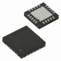
ATTINY84-20MUR Atmel, ATTINY84-20MUR Datasheet - Page 150

ATTINY84-20MUR
Manufacturer Part Number
ATTINY84-20MUR
Description
MCU AVR 8KB FLASH 20MHZ 20QFN
Manufacturer
Atmel
Series
AVR® ATtinyr
Specifications of ATTINY84-20MUR
Core Processor
AVR
Core Size
8-Bit
Speed
20MHz
Connectivity
USI
Peripherals
Brown-out Detect/Reset, POR, PWM, Temp Sensor, WDT
Number Of I /o
12
Program Memory Size
8KB (4K x 16)
Program Memory Type
FLASH
Eeprom Size
512 x 8
Ram Size
512 x 8
Voltage - Supply (vcc/vdd)
2.7 V ~ 5.5 V
Data Converters
A/D 8x10b
Oscillator Type
Internal
Operating Temperature
-40°C ~ 85°C
Package / Case
*
Lead Free Status / RoHS Status
Lead free / RoHS Compliant
- Current page: 150 of 238
- Download datasheet (5Mb)
16.13.5
150
ATtiny24/44/84
DIDR0 – Digital Input Disable Register 0
• Bit 6 – ACME: Analog Comparator Multiplexer Enable
See
• Bit 5 – Res: Reserved Bit
This is a reserved bit in ATtiny24/44/84. For compatibility with future devices always write this bit
to zero.
• Bit 4 – ADLAR: ADC Left Adjust Result
The ADLAR bit affects the presentation of the ADC conversion result in the ADC Data Register.
Write one to ADLAR to left adjust the result. Otherwise, the result is right adjusted. Changing the
ADLAR bit will affect the ADC Data Register immediately, regardless of any ongoing conver-
sions. For a comple the description of this bit, see
page
• Bit 3 – Res: Reserved Bit
This bit is reserved bit in the ATtiny24/44/84 and will always read as what was wrote there.
• Bits 2:0 – ADTS2:0: ADC Auto Trigger Source
If ADATE in ADCSRA is written to one, the value of these bits selects which source will trigger
an ADC conversion. If ADATE is cleared, the ADTS2:0 settings will have no effect. A conversion
will be triggered by the rising edge of the selected Interrupt Flag. Note that switching from a trig-
ger source that is cleared to a trigger source that is set, will generate a positive edge on the
trigger signal. If ADEN in ADCSRA is set, this will start a conversion. Switching to Free Running
mode (ADTS[2:0]=0) will not cause a trigger event, even if the ADC Interrupt Flag is set
Table 16-7.
• Bits 7:0 – ADC7D:ADC0D: ADC7:0 Digital Input Disable
When a bit is written logic one, the digital input buffer on the corresponding ADC pin is disabled.
The corresponding PIN register bit will always read as zero when this bit is set. When an analog
signal is applied to the ADC7:0 pin and the digital input from this pin is not needed, this bit
should be written logic one to reduce power consumption in the digital input buffer.
Bit
0x01 (0x21)
Read/Write
Initial Value
“ADCSRB – ADC Control and Status Register B” on page
149.
ADTS2
0
0
0
0
1
1
1
1
ADC Auto Trigger Source Selections
ADC7D
R/W
7
0
ADC6D
ADTS1
R/W
6
0
0
0
1
1
0
0
1
1
ADC5D
R/W
5
0
ADC4D
R/W
ADTS0
4
0
0
1
0
1
0
1
0
1
“ADCL and ADCH – ADC Data Register” on
ADC3D
R/W
3
0
Trigger Source
Free Running mode
Analog Comparator
External Interrupt Request 0
Timer/Counter0 Compare Match A
Timer/Counter0 Overflow
Timer/Counter1 Compare Match B
Timer/Counter1 Overflow
Timer/Counter1 Capture Event
ADC2D
R/W
2
0
131.
ADC1D
R/W
1
0
ADC0D
R/W
0
0
8006K–AVR–10/10
.
DIDR0
Related parts for ATTINY84-20MUR
Image
Part Number
Description
Manufacturer
Datasheet
Request
R

Part Number:
Description:
Manufacturer:
Atmel Corporation
Datasheet:

Part Number:
Description:
Manufacturer:
Atmel Corporation
Datasheet:

Part Number:
Description:
IC MCU AVR 8K FLASH 20MHZ 20-QFN
Manufacturer:
Atmel
Datasheet:

Part Number:
Description:
MCU AVR 8K ISP FLASH 2.7V 14SOIC
Manufacturer:
Atmel
Datasheet:

Part Number:
Description:
MCU AVR 8K FLASH 15MHZ 20-QFN
Manufacturer:
Atmel
Datasheet:

Part Number:
Description:
IC MCU AVR 8K FLASH 20MHZ 14-DIP
Manufacturer:
Atmel
Datasheet:

Part Number:
Description:
MCU AVR 8KB FLASH 10MHZ 14SOIC
Manufacturer:
Atmel
Datasheet:

Part Number:
Description:
IC, MCU, 8BIT, 2K FLASH, 20SOIC
Manufacturer:
Atmel
Datasheet:

Part Number:
Description:
IC, MCU, 8BIT, 2K FLASH, 20PDIP
Manufacturer:
Atmel
Datasheet:

Part Number:
Description:
IC, MCU, 8BIT, 8K FLASH, 20PDIP
Manufacturer:
Atmel
Datasheet:

Part Number:
Description:
IC, MCU, 8BIT, 8K FLASH, 20SOIC
Manufacturer:
Atmel
Datasheet:

Part Number:
Description:
DEV KIT FOR AVR/AVR32
Manufacturer:
Atmel
Datasheet:

Part Number:
Description:
INTERVAL AND WIPE/WASH WIPER CONTROL IC WITH DELAY
Manufacturer:
ATMEL Corporation
Datasheet:

Part Number:
Description:
Low-Voltage Voice-Switched IC for Hands-Free Operation
Manufacturer:
ATMEL Corporation
Datasheet:


