PIC16F685-E/P Microchip Technology, PIC16F685-E/P Datasheet - Page 28
PIC16F685-E/P
Manufacturer Part Number
PIC16F685-E/P
Description
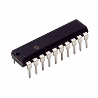
IC PIC MCU FLASH 4KX14 20DIP
Manufacturer
Microchip Technology
Series
PIC® 16Fr
Datasheets
1.PIC16F616T-ISL.pdf
(8 pages)
2.PIC16F690DM-PCTLHS.pdf
(306 pages)
3.PIC16F677-IP.pdf
(2 pages)
4.PIC16F677-IP.pdf
(16 pages)
Specifications of PIC16F685-E/P
Core Processor
PIC
Core Size
8-Bit
Speed
20MHz
Peripherals
Brown-out Detect/Reset, POR, PWM, WDT
Number Of I /o
18
Program Memory Size
7KB (4K x 14)
Program Memory Type
FLASH
Eeprom Size
256 x 8
Ram Size
256 x 8
Voltage - Supply (vcc/vdd)
2 V ~ 5.5 V
Data Converters
A/D 12x10b
Oscillator Type
Internal
Operating Temperature
-40°C ~ 125°C
Package / Case
20-DIP (0.300", 7.62mm)
For Use With
AC162061 - HEADER INTRFC MPLAB ICD2 20PINAC164039 - MODULE SKT PROMATE II 20DIP/SOICDM163029 - BOARD PICDEM FOR MECHATRONICSACICE0203 - MPLABICE 20P 300 MIL ADAPTER
Lead Free Status / RoHS Status
Lead free / RoHS Compliant
Connectivity
-


PIC16F631/677/685/687/689/690
2.2
The data memory (see Figures 2-6 through 2-8) is
partitioned into four banks which contain the General
Purpose Registers (GPR) and the Special Function
Registers (SFR). The Special Function Registers are
located in the first 32 locations of each bank. The
General Purpose Registers, implemented as static
RAM, are located in the last 96 locations of each Bank.
Register locations F0h-FFh in Bank 1, 170h-17Fh in
Bank 2 and 1F0h-1FFh in Bank 3 point to addresses
70h-7Fh in Bank 0. The actual number of General
Purpose Resisters (GPR) in each Bank depends on the
device. Details are shown in Figures 2-4 through 2-8.
All other RAM is unimplemented and returns ‘0’ when
read. RP<1:0> of the STATUS register are the bank
select bits:
RP1
2.2.1
The register file is organized as 128 x 8 in the
PIC16F687
PIC16F685/PIC16F689/PIC16F690. Each register is
accessed, either directly or indirectly, through the File
Select Register (FSR) (see Section 2.4 “Indirect
Addressing, INDF and FSR Registers”).
2.2.2
The Special Function Registers are registers used by
the CPU and peripheral functions for controlling the
desired operation of the device (see Tables 2-1
through 2-4). These registers are static RAM.
The special registers can be classified into two sets:
core and peripheral. The Special Function Registers
associated with the “core” are described in this section.
Registers related to the operation of peripheral features
are described in the section of that peripheral feature.
DS41262E-page 26
0
0
1
1
RP0
0
1
0
1
Data Memory Organization
GENERAL PURPOSE REGISTER
FILE
SPECIAL FUNCTION REGISTERS
→
→
→
→
and
Bank 0 is selected
Bank 1 is selected
Bank 2 is selected
Bank 3 is selected
256
x
8
in
the
© 2008 Microchip Technology Inc.
Related parts for PIC16F685-E/P
Image
Part Number
Description
Manufacturer
Datasheet
Request
R

Part Number:
Description:
3.5KB Flash, 128B RAM, 18 I/O, CLC, CWG, DDS, 10-bit ADC 20 QFN 4x4mm TUBE
Manufacturer:
Microchip Technology
Datasheet:

Part Number:
Description:
3.5KB Flash, 128B RAM, 18 I/O, CLC, CWG, DDS, 10-bit ADC 20 PDIP .300in TUBE
Manufacturer:
Microchip Technology
Datasheet:

Part Number:
Description:
3.5KB Flash, 128B RAM, 18 I/O, CLC, CWG, DDS, 10-bit ADC 20 SOIC .300in TUBE
Manufacturer:
Microchip Technology
Datasheet:

Part Number:
Description:
3.5KB Flash, 128B RAM, 18 I/O, CLC, CWG, DDS, 10-bit ADC 20 SSOP .209in TUBE
Manufacturer:
Microchip Technology
Datasheet:
Part Number:
Description:
3.5KB Flash, 128B RAM, 18 I/O, CLC, CWG, DDS, 10-bit ADC 20 QFN 4x4mm TUBE
Manufacturer:
Microchip Technology
Datasheet:
Part Number:
Description:
3.5KB Flash, 128B RAM, 18 I/O, CLC, CWG, DDS, 10-bit ADC 20 PDIP .300in TUBE
Manufacturer:
Microchip Technology
Datasheet:
Part Number:
Description:
3.5KB Flash, 128B RAM, 18 I/O, CLC, CWG, DDS, 10-bit ADC 20 SOIC .300in TUBE
Manufacturer:
Microchip Technology
Datasheet:
Part Number:
Description:
3.5KB Flash, 128B RAM, 18 I/O, CLC, CWG, DDS, 10-bit ADC 20 SSOP .209in TUBE
Manufacturer:
Microchip Technology
Datasheet:
Part Number:
Description:
3.5KB Flash, 128B RAM, 18 I/O, CLC, CWG, DDS, 10-bit ADC 20 QFN 4x4mm T/R
Manufacturer:
Microchip Technology
Datasheet:
Part Number:
Description:
3.5KB Flash, 128B RAM, 18 I/O, CLC, CWG, DDS, 10-bit ADC 20 SOIC .300in T/R
Manufacturer:
Microchip Technology
Datasheet:
Part Number:
Description:
3.5KB Flash, 128B RAM, 18 I/O, CLC, CWG, DDS, 10-bit ADC 20 SSOP .209in T/R
Manufacturer:
Microchip Technology
Datasheet:
Part Number:
Description:
3.5KB Flash, 128B RAM, 18 I/O, CLC, CWG, DDS, 10-bit ADC 20 QFN 4x4mm TUBE
Manufacturer:
Microchip Technology
Datasheet:
Part Number:
Description:
3.5KB Flash, 128B RAM, 18 I/O, CLC, CWG, DDS, 10-bit ADC 20 PDIP .300in TUBE
Manufacturer:
Microchip Technology
Datasheet:
Part Number:
Description:
3.5KB Flash, 128B RAM, 18 I/O, CLC, CWG, DDS, 10-bit ADC 20 SOIC .300in TUBE
Manufacturer:
Microchip Technology
Datasheet:
Part Number:
Description:
3.5KB Flash, 128B RAM, 18 I/O, CLC, CWG, DDS, 10-bit ADC 20 SSOP .209in TUBE
Manufacturer:
Microchip Technology
Datasheet: