ATTINY43U-MUR Atmel, ATTINY43U-MUR Datasheet - Page 20
ATTINY43U-MUR
Manufacturer Part Number
ATTINY43U-MUR
Description
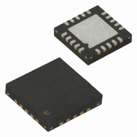
MCU AVR 4KB FLASH 8MHZ 20QFN
Manufacturer
Atmel
Series
AVR® ATtinyr
Specifications of ATTINY43U-MUR
Core Processor
AVR
Core Size
8-Bit
Speed
8MHz
Connectivity
USI
Peripherals
Brown-out Detect/Reset, POR, PWM, Temp Sensor, WDT
Number Of I /o
16
Program Memory Size
4KB (2K x 16)
Program Memory Type
FLASH
Eeprom Size
64 x 8
Ram Size
256 x 8
Voltage - Supply (vcc/vdd)
1.8 V ~ 5.5 V
Data Converters
A/D 4x10b
Oscillator Type
Internal
Operating Temperature
-40°C ~ 85°C
Package / Case
*
Lead Free Status / RoHS Status
Lead free / RoHS Compliant


5.5
5.5.1
5.6
5.6.1
20
I/O Memory
Register Description
ATtiny43U
General Purpose I/O Registers
EEAR – EEPROM Address Register
The I/O space definition of the ATtiny43U is shown in
All I/Os and peripherals are placed in the I/O space. All I/O locations may be accessed by the
LD/LDS/LDD and ST/STS/STD instructions, transferring data between the 32 general purpose
working registers and the I/O space. I/O Registers within the address range 0x00 - 0x1F are
directly bit-accessible using the SBI and CBI instructions. In these registers, the value of single
bits can be checked by using the SBIS and SBIC instructions. See the instruction set section for
more details. When using the I/O specific commands IN and OUT, the I/O addresses 0x00 -
0x3F must be used. When addressing I/O Registers as data space using LD and ST instruc-
tions, 0x20 must be added to these addresses.
For compatibility with future devices, reserved bits should be written to zero if accessed.
Reserved I/O memory addresses should never be written.
Some of the Status Flags are cleared by writing a logical one to them. Note that, unlike most
other AVRs, the CBI and SBI instructions will only operate on the specified bit, and can therefore
be used on registers containing such Status Flags. The CBI and SBI instructions work with reg-
isters 0x00 to 0x1F only.
The I/O and Peripherals Control Registers are explained in later sections.
ATtiny43U contains three General Purpose I/O Registers. These registers can be used for stor-
ing any information, and they are particularly useful for storing global variables and status flags.
General Purpose I/O Registers within the address range 0x00 - 0x1F are directly bit-accessible
using the SBI, CBI, SBIS, and SBIC instructions.
• Bits 7:6 – Res: Reserved Bit
These bits are reserved and will always read zero.
• Bits 5:0 – EEAR[5:0]: EEPROM Address
The EEPROM Address Register – EEAR – specifies the EEPROM address. The EEPROM data
bytes are addressed linearly in the range 0...(64-1). The initial value of EEAR is undefined. A
proper value must be written before the EEPROM may be accessed.
Bit
0x1E (0x3E)
Read/Write
Initial Value
R
7
0
-
R
6
0
-
EEAR5
R/W
5
X
EEAR4
R/W
X
4
EEAR3
R/W
X
3
“Register Summary” on page
EEAR2
R/W
2
X
EEAR1
R/W
X
1
EEAR0
R/W
X
0
8048B–AVR–03/09
167.
EEAR
Related parts for ATTINY43U-MUR
Image
Part Number
Description
Manufacturer
Datasheet
Request
R

Part Number:
Description:
Manufacturer:
Atmel Corporation
Datasheet:

Part Number:
Description:
Microcontrollers (MCU) 512B FL 32B SRAM TIMER ATTINY4 12MHz
Manufacturer:
Atmel
Part Number:
Description:
IC MCU AVR 512B FLASH SOT-23-6
Manufacturer:
Atmel
Datasheet:

Part Number:
Description:
IC MCU AVR 512B FLASH SOT-23-6
Manufacturer:
Atmel
Datasheet:

Part Number:
Description:
DEV KIT FOR AVR/AVR32
Manufacturer:
Atmel
Datasheet:
Part Number:
Description:
INTERVAL AND WIPE/WASH WIPER CONTROL IC WITH DELAY
Manufacturer:
ATMEL Corporation
Datasheet:
Part Number:
Description:
Low-Voltage Voice-Switched IC for Hands-Free Operation
Manufacturer:
ATMEL Corporation
Datasheet:
Part Number:
Description:
MONOLITHIC INTEGRATED FEATUREPHONE CIRCUIT
Manufacturer:
ATMEL Corporation
Datasheet:
Part Number:
Description:
AM-FM Receiver IC U4255BM-M
Manufacturer:
ATMEL Corporation
Datasheet:
Part Number:
Description:
Monolithic Integrated Feature Phone Circuit
Manufacturer:
ATMEL Corporation
Datasheet:
Part Number:
Description:
Multistandard Video-IF and Quasi Parallel Sound Processing
Manufacturer:
ATMEL Corporation
Datasheet: