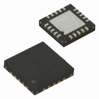
ATTINY4313-MU Atmel, ATTINY4313-MU Datasheet - Page 64

ATTINY4313-MU
Manufacturer Part Number
ATTINY4313-MU
Description
IC MCU AVR 4K FLASH 20QFN
Manufacturer
Atmel
Series
AVR® ATtinyr
Specifications of ATTINY4313-MU
Core Processor
AVR
Core Size
8-Bit
Speed
20MHz
Connectivity
I²C, SPI, UART/USART
Peripherals
Brown-out Detect/Reset, POR, PWM, WDT
Number Of I /o
18
Program Memory Size
4KB (2K x 16)
Program Memory Type
FLASH
Eeprom Size
256 x 8
Ram Size
256 x 8
Voltage - Supply (vcc/vdd)
1.8 V ~ 5.5 V
Oscillator Type
Internal
Operating Temperature
-40°C ~ 85°C
Package / Case
20-VQFN Exposed Pad, 20-HVQFN, 20-SQFN, 20-DHVQFN
Processor Series
ATtiny
Core
AVR
Data Bus Width
8 bit
Data Ram Size
256 B
Interface Type
SPI, USART, USI
Maximum Clock Frequency
20 MHz
Number Of Programmable I/os
18
Number Of Timers
2
Operating Supply Voltage
3.3 V
Maximum Operating Temperature
+ 85 C
Mounting Style
SMD/SMT
Minimum Operating Temperature
- 40 C
Operating Temperature Range
- 40 C to + 85 C
Lead Free Status / RoHS Status
Lead free / RoHS Compliant
Data Converters
-
Lead Free Status / Rohs Status
Details
Available stocks
Company
Part Number
Manufacturer
Quantity
Price
Company:
Part Number:
ATTINY4313-MU
Manufacturer:
HITTITE
Quantity:
101
- Current page: 64 of 270
- Download datasheet (7Mb)
64
ATtiny2313A/4313
• Port B, Bit 5 – DI/SDA/PCINT5
• Port B, Bit 6 – DO/PCINT6
• Port B, Bit 7 – USCK/SCL/PCINT7
Table 10-6
shown in
MISO signal, while MOSI is divided into SPI MSTR OUTPUT and SPI SLAVE INPUT.
• PCINT4: Pin Change Interrupt Source 4. The PB4 pin can serve as an external interrupt
• DI: Three-wire mode Universal Serial Interface Data input. Three-wire mode does not
• PCINT5: Pin Change Interrupt Source 5. The PB5 pin can serve as an external interrupt
• DO: Three-wire mode Universal Serial Interface Data output. Three-wire mode Data output
• PCINT6: Pin Change Interrupt Source 6. The PB6 pin can serve as an external interrupt
• USCK: Three-wire mode Universal Serial Interface Clock.
• SCL: Two-wire mode Serial Clock for USI Two-wire mode.
• PCINT7: Pin Change Interrupt source 7. The PB7 pin can serve as an external interrupt
(one)) to serve this function. The OC1B pin is also the output pin for the PWM mode timer
function.
source for pin change interrupt 0.
override normal port functions, so pin must be configured as an input. SDA: Two-wire mode
Serial Interface Data.
source for pin change interrupt 0.
overrides PORTB6 value and it is driven to the port when data direction bit DDB6 is set (one).
However the PORTB6 bit still controls the pull-up enabling pull-up, if direction is input and
PORTB6 is set (one).
source for pin change interrupt 0.
source for pin change interrupt 0.
Figure 10-5 on page
and
Table 10-7
relate the alternate functions of Port B to the overriding signals
59. SPI MSTR INPUT and SPI SLAVE OUTPUT constitute the
8246A–AVR–11/09
Related parts for ATTINY4313-MU
Image
Part Number
Description
Manufacturer
Datasheet
Request
R

Part Number:
Description:
Manufacturer:
Atmel Corporation
Datasheet:

Part Number:
Description:
Microcontrollers (MCU) 512B FL 32B SRAM TIMER ATTINY4 12MHz
Manufacturer:
Atmel

Part Number:
Description:
IC MCU AVR 512B FLASH SOT-23-6
Manufacturer:
Atmel
Datasheet:

Part Number:
Description:
IC MCU AVR 512B FLASH SOT-23-6
Manufacturer:
Atmel
Datasheet:

Part Number:
Description:
DEV KIT FOR AVR/AVR32
Manufacturer:
Atmel
Datasheet:

Part Number:
Description:
INTERVAL AND WIPE/WASH WIPER CONTROL IC WITH DELAY
Manufacturer:
ATMEL Corporation
Datasheet:

Part Number:
Description:
Low-Voltage Voice-Switched IC for Hands-Free Operation
Manufacturer:
ATMEL Corporation
Datasheet:

Part Number:
Description:
MONOLITHIC INTEGRATED FEATUREPHONE CIRCUIT
Manufacturer:
ATMEL Corporation
Datasheet:

Part Number:
Description:
AM-FM Receiver IC U4255BM-M
Manufacturer:
ATMEL Corporation
Datasheet:

Part Number:
Description:
Monolithic Integrated Feature Phone Circuit
Manufacturer:
ATMEL Corporation
Datasheet:

Part Number:
Description:
Multistandard Video-IF and Quasi Parallel Sound Processing
Manufacturer:
ATMEL Corporation
Datasheet:


