ATTINY20-XU Atmel, ATTINY20-XU Datasheet - Page 93
ATTINY20-XU
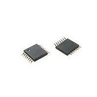
Manufacturer Part Number
ATTINY20-XU
Description
MCU AVR 2KB FLASH 12MHZ 14TSSOP
Manufacturer
Atmel
Series
AVR® ATtinyr
Datasheet
1.ATTINY20-EK1.pdf
(224 pages)
Specifications of ATTINY20-XU
Core Processor
AVR
Core Size
8-Bit
Speed
12MHz
Connectivity
I²C, SPI
Peripherals
Brown-out Detect/Reset, POR, PWM, WDT
Number Of I /o
12
Program Memory Size
2KB (1K x 16)
Program Memory Type
FLASH
Ram Size
128 x 8
Voltage - Supply (vcc/vdd)
1.8 V ~ 5.5 V
Data Converters
A/D 8x10b
Oscillator Type
Internal
Operating Temperature
-40°C ~ 85°C
Package / Case
*
Processor Series
ATtiny
Core
AVR
Data Bus Width
8 bit
Data Ram Size
128 B
Interface Type
SPI, TWI
Maximum Clock Frequency
12 MHz
Number Of Programmable I/os
12
Number Of Timers
2
Operating Supply Voltage
3.3 V
Maximum Operating Temperature
+ 85 C
Mounting Style
SMD/SMT
Minimum Operating Temperature
- 40 C
Operating Temperature Range
- 40 C to + 85 C
Lead Free Status / RoHS Status
Lead free / RoHS Compliant
Eeprom Size
-
Lead Free Status / Rohs Status
Details
Available stocks
Company
Part Number
Manufacturer
Quantity
Price
Company:

Part Number:
ATTINY20-XU
Manufacturer:
Atmel
Quantity:
904


12.9
8235B–AVR–04/11
Timer/Counter Timing Diagrams
When changing the TOP value the program must ensure that the new TOP value is higher or
equal to the value of all of the Compare Registers. If the TOP value is lower than any of the
Compare Registers, a compare match will never occur between the TCNT1 and the OCR1x.
As
cal in all periods. Since the OCR1x Registers are updated at BOTTOM, the length of the rising
and the falling slopes will always be equal. This gives symmetrical output pulses and is therefore
frequency correct.
Using the ICR1 Register for defining TOP works well when using fixed TOP values. By using
ICR1, the OCR1A Register is free to be used for generating a PWM output on OC1A. However,
if the base PWM frequency is actively changed by changing the TOP value, using the OCR1A as
TOP is clearly a better choice due to its double buffer feature.
In phase and frequency correct PWM mode, the compare units allow generation of PWM wave-
forms on the OC1x pins. Setting the COM1x[1:0] bits to two will produce a non-inverted PWM
and an inverted PWM output can be generated by setting the COM1x[1:0] to three (See
12-4 on page
for the port pin is set as output (DDR_OC1x). The PWM waveform is generated by setting (or
clearing) the OC1x Register at the compare match between OCR1x and TCNT1 when the coun-
ter increments, and clearing (or setting) the OC1x Register at compare match between OCR1x
and TCNT1 when the counter decrements. The PWM frequency for the output when using
phase and frequency correct PWM can be calculated by the following equation:
The N variable represents the prescaler divider (1, 8, 64, 256, or 1024).
The extreme values for the OCR1x Register represents special cases when generating a PWM
waveform output in the phase correct PWM mode. If the OCR1x is set equal to BOTTOM the
output will be continuously low and if set equal to TOP the output will be set to high for non-
inverted PWM mode. For inverted PWM the output will have the opposite logic values.
The Timer/Counter is a synchronous design and the timer clock (clk
clock enable signal in the following figures. The figures include information on when interrupt
flags are set, and when the OCR1x Register is updated with the OCR1x buffer value (only for
modes utilizing double buffering).
Figure 12-9
100). The actual OC1x value will only be visible on the port pin if the data direction
shows the output generated is, in contrast to the phase correct mode, symmetri-
f
OCnxPFCPWM
Figure 12-10
shows a timing diagram for the setting of OCF1x.
=
--------------------------- -
2 N TOP
⋅
f
clk_I/O
⋅
T1
) is therefore shown as a
ATtiny20
Table
93
Related parts for ATTINY20-XU
Image
Part Number
Description
Manufacturer
Datasheet
Request
R

Part Number:
Description:
IC, MCU, 8BIT, 2K FLASH, 20SOIC
Manufacturer:
Atmel
Datasheet:

Part Number:
Description:
IC, MCU, 8BIT, 2K FLASH, 20PDIP
Manufacturer:
Atmel
Datasheet:
Part Number:
Description:
IC, MCU, 8BIT, 8K FLASH, 20PDIP
Manufacturer:
Atmel
Datasheet:
Part Number:
Description:
IC, MCU, 8BIT, 8K FLASH, 20SOIC
Manufacturer:
Atmel
Datasheet:

Part Number:
Description:
DEV KIT FOR AVR/AVR32
Manufacturer:
Atmel
Datasheet:

Part Number:
Description:
INTERVAL AND WIPE/WASH WIPER CONTROL IC WITH DELAY
Manufacturer:
ATMEL Corporation
Datasheet:
Part Number:
Description:
Low-Voltage Voice-Switched IC for Hands-Free Operation
Manufacturer:
ATMEL Corporation
Datasheet:
Part Number:
Description:
MONOLITHIC INTEGRATED FEATUREPHONE CIRCUIT
Manufacturer:
ATMEL Corporation
Datasheet:
Part Number:
Description:
AM-FM Receiver IC U4255BM-M
Manufacturer:
ATMEL Corporation
Datasheet:
Part Number:
Description:
Monolithic Integrated Feature Phone Circuit
Manufacturer:
ATMEL Corporation
Datasheet:
Part Number:
Description:
Multistandard Video-IF and Quasi Parallel Sound Processing
Manufacturer:
ATMEL Corporation
Datasheet:
Part Number:
Description:
High-performance EE PLD
Manufacturer:
ATMEL Corporation
Datasheet: