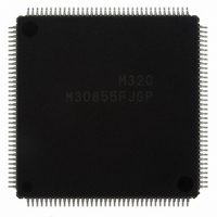
M30855FJGP#U3 Renesas Electronics America, M30855FJGP#U3 Datasheet - Page 90

M30855FJGP#U3
Manufacturer Part Number
M30855FJGP#U3
Description
IC M32C MCU FLASH 512K 144LQFP
Manufacturer
Renesas Electronics America
Series
M16C™ M32C/80r
Specifications of M30855FJGP#U3
Core Processor
M32C/80
Core Size
16/32-Bit
Speed
32MHz
Connectivity
CAN, I²C, IEBus, SIO, UART/USART
Peripherals
DMA, WDT
Number Of I /o
121
Program Memory Size
512KB (512K x 8)
Program Memory Type
FLASH
Ram Size
24K x 8
Voltage - Supply (vcc/vdd)
3 V ~ 5.5 V
Data Converters
A/D 34x10b, D/A 2x8b
Oscillator Type
Internal
Operating Temperature
-40°C ~ 85°C
Package / Case
144-LQFP
For Use With
R0K330879S001BE - KIT DEV RSK M32C/87R0K330879S000BE - KIT DEV RSK M32C/87
Lead Free Status / RoHS Status
Lead free / RoHS Compliant
Eeprom Size
-
Available stocks
Company
Part Number
Manufacturer
Quantity
Price
0.52 Mar.12, 2004
Rev.
0.30 Jul.18, 2003
0.40 Sep.30, 2003
0.50 Feb.05, 2004
0.51 Feb.09, 2004
Date
REVISION HISTORY
7, 11, 12 • Figures 1.4 to 1.6 Pin Assignments Note 2 added
16 to 18 - SDA0 to SDA4 pins changed from output pins to I/O pins.
2 to 3
10,14
44,45
Page
2, 3
2, 3
17
18
19
23
24
52
59
60
70
71
–
5
6
New Document
Overview
• Tables 1.1 and 1.2 M32C/85 Performance “Oscillator Stop Detect Function”
• Figure 1.2 ROM/RAM Capacity and Table 1.3. M32C/85 Group M30852ME-
• ROM capacity “192 Kbytes” deleted
- V
- TA4
- TA4
- ISRxD1 pin modified to ISRxD0 pin in port P8.
- DA0 and DA1 pins changed from input pins to output pins.
- Symbol “P11
- Descriptions of ISTxD1 and BE1
SFR
- Notes written directly in the Tables.
Overview
• Tables 1.1 and 1.2 M32C/85 Performance “Shortest Instruction Execution
Memory
• Figure 3.1 Memory Map Diagram modified
SFR
• “After RESET” values of PM 1, PM 2, D4INT, G0IRF, G1IRF, IDB0 to IDB1,
• NOTES added to PM0 and TCSPR registers
Electrical Characteristics
• Newly added
Electrical Characteristics
• Table 5.6 Flash Memory Version Electrical Characteristics Note 4 changed
• Figure 5.2 V
• Figure 5.3 V
• Figure 5.6 V
• Figure 5.7 V
Overview
• Table 1.1 and 1.2 M32C/85 Group Performance Value of Power Consump-
added
XXXGP and M30850ME-XXXGP/FP deleted
data”.
Time” and “Power Comsumption” values modified
TA0MR to TA4MR, TCSPR, DM0SL to DM3SL registers corrected
tion modified
REF
OUT
IN
pin changed from analog input pins to control pins.
pin changed from output pin to input pin.
changed from input pin to I/O pin.
CC
7
CC
CC
CC
” modified to “P11
1=V
1=V
1=V
1=V
M32C/85 Group (M32C/85, M32C/85T) Datasheet
CC
CC
CC
CC
A-1
2=5V Timing Diagram (1) Notes 1 and 2 changed
2=5V Timing Diagram (2) Notes 1, 2, and 3 changed
2=3.3V Timing Diagram (1) Notes 1, 2, and 3 changed
2=3.3V Timing Diagram (2) Notes 1 and 2 changed
Description
4
” and description from “8-bit” to “5-bit”.
IN
Summary
modified from “received data” to “transmit


