M30879FKBGP#U5 Renesas Electronics America, M30879FKBGP#U5 Datasheet - Page 92
M30879FKBGP#U5
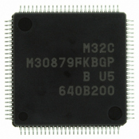
Manufacturer Part Number
M30879FKBGP#U5
Description
IC M32C/87 MCU FLASH 100LQFP
Manufacturer
Renesas Electronics America
Series
M16C™ M32C/80r
Datasheet
1.M3087BFLGPU3.pdf
(629 pages)
Specifications of M30879FKBGP#U5
Core Processor
M32C/80
Core Size
16/32-Bit
Speed
32MHz
Connectivity
EBI/EMI, I²C, IEBus, IrDA, SIO, UART/USART
Peripherals
DMA, POR, PWM, WDT
Number Of I /o
85
Program Memory Size
768KB (768K x 8)
Program Memory Type
FLASH
Ram Size
48K x 8
Voltage - Supply (vcc/vdd)
3 V ~ 5.5 V
Data Converters
A/D 26x10b; D/A 2x8b
Oscillator Type
Internal
Operating Temperature
-20°C ~ 85°C
Package / Case
100-LQFP
For Use With
R0K330879S001BE - KIT DEV RSK M32C/87R0K330879S000BE - KIT DEV RSK M32C/87
Lead Free Status / RoHS Status
Lead free / RoHS Compliant
Eeprom Size
-
Available stocks
Company
Part Number
Manufacturer
Quantity
Price

Part Number:
M30879FKBGP#U5M30879FKBGP#U3
Manufacturer:
Renesas Electronics America
Quantity:
10 000


M32C/87 Group (M32C/87, M32C/87A, M32C/87B)
REJ09B0180-0151 Rev.1.51 Jul 31, 2008
Page 68 of 587
8.2.3
Table 8.4
NOTE:
Table 8.5
Data Bus Width
16 bits
8 bits
Data Bus Width
16 bits
8 bits
1. These become WR output.
When using a 16-bit data bus, the PM02 bit in the PM0 register selects either a combination of the “RD, WR,
and BHE” outputs or the “RD, WRL, and WRH” outputs to determine the read/write output signals. When bits
DS3 to DS0 in the DS register are set to 0 (8-bit external data bus width), set the PM02 bit to 0 (RD/WR/BHE).
When any of bits DS3 to DS0 is set to 1 (16-bit external data bus width) to access an 8-bit space, the
combination of “RD, WR, and BHE” is automatically selected regardless of the PM02 bit setting. Table 8.4 lists
RD, WRL, and WRH outputs. Table 8.5 list RD, WR, and BHE outputs.
The RD, WR, and BHE outputs are selected for the read/write output signals after reset. When changing to
“RD, WRL, and WRH” outputs, set the PM02 bit first to write data to an external memory.
Read/Write Output Signals
RD, WRL, and WRH Outputs
RD, WR, and BHE Outputs
RD
RD
H
H
H
H
H
H
H
H
L
L
L
L
L
L
WRL
H
WR
L
H
H
H
H
H
H
L
L
L
L
L
L
(1)
(1)
Not used
Not used
Not used
Not used
WRH
BHE
H
H
H
H
L
L
L
L
L
L
Not used
Not used
Not used
Not used
H/L
H/L
H/L
H/L
A0
A0
H
H
L
L
L
L
Read data
Write 1-byte data to even address
Write 1-byte data to odd address
Write data to both even and odd addresses
Write 1-byte data
Read 1-byte data
Write 1-byte data to odd address
Read 1-byte data from odd address
Write 1-byte data to even address
Read 1-byte data from even address
Write data to both even and odd addresses
Read data from both even and odd addresses
Write 1-byte data
Read 1-byte data
CPU Processing on External Space
CPU Processing on External Space
8. Bus
Related parts for M30879FKBGP#U5
Image
Part Number
Description
Manufacturer
Datasheet
Request
R

Part Number:
Description:
KIT STARTER FOR M16C/29
Manufacturer:
Renesas Electronics America
Datasheet:

Part Number:
Description:
KIT STARTER FOR R8C/2D
Manufacturer:
Renesas Electronics America
Datasheet:

Part Number:
Description:
R0K33062P STARTER KIT
Manufacturer:
Renesas Electronics America
Datasheet:

Part Number:
Description:
KIT STARTER FOR R8C/23 E8A
Manufacturer:
Renesas Electronics America
Datasheet:

Part Number:
Description:
KIT STARTER FOR R8C/25
Manufacturer:
Renesas Electronics America
Datasheet:

Part Number:
Description:
KIT STARTER H8S2456 SHARPE DSPLY
Manufacturer:
Renesas Electronics America
Datasheet:

Part Number:
Description:
KIT STARTER FOR R8C38C
Manufacturer:
Renesas Electronics America
Datasheet:

Part Number:
Description:
KIT STARTER FOR R8C35C
Manufacturer:
Renesas Electronics America
Datasheet:

Part Number:
Description:
KIT STARTER FOR R8CL3AC+LCD APPS
Manufacturer:
Renesas Electronics America
Datasheet:
Part Number:
Description:
KIT STARTER FOR RX610
Manufacturer:
Renesas Electronics America
Datasheet:

Part Number:
Description:
KIT STARTER FOR R32C/118
Manufacturer:
Renesas Electronics America
Datasheet:

Part Number:
Description:
KIT DEV RSK-R8C/26-29
Manufacturer:
Renesas Electronics America
Datasheet:

Part Number:
Description:
KIT STARTER FOR SH7124
Manufacturer:
Renesas Electronics America
Datasheet:

Part Number:
Description:
KIT STARTER FOR H8SX/1622
Manufacturer:
Renesas Electronics America
Datasheet:

Part Number:
Description:
KIT DEV FOR SH7203
Manufacturer:
Renesas Electronics America
Datasheet: