M30873FHBGP#U3 Renesas Electronics America, M30873FHBGP#U3 Datasheet - Page 283
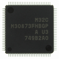
M30873FHBGP#U3
Manufacturer Part Number
M30873FHBGP#U3
Description
IC M32C/87 MCU FLASH 100LQFP
Manufacturer
Renesas Electronics America
Series
M16C™ M32C/80r
Datasheet
1.M3087BFLGPU3.pdf
(629 pages)
Specifications of M30873FHBGP#U3
Core Processor
M32C/80
Core Size
16/32-Bit
Speed
32MHz
Connectivity
EBI/EMI, I²C, IEBus, IrDA, SIO, UART/USART
Peripherals
DMA, POR, PWM, WDT
Number Of I /o
85
Program Memory Size
384KB (384K x 8)
Program Memory Type
FLASH
Ram Size
24K x 8
Voltage - Supply (vcc/vdd)
3 V ~ 5.5 V
Data Converters
A/D 26x10b; D/A 2x8b
Oscillator Type
Internal
Operating Temperature
-40°C ~ 85°C
Package / Case
100-LQFP
For Use With
R0K330879S001BE - KIT DEV RSK M32C/87R0K330879S000BE - KIT DEV RSK M32C/87
Lead Free Status / RoHS Status
Lead free / RoHS Compliant
Eeprom Size
-
Available stocks
Company
Part Number
Manufacturer
Quantity
Price


M32C/87 Group (M32C/87, M32C/87A, M32C/87B)
REJ09B0180-0151 Rev.1.51 Jul 31, 2008
Page 259 of 587
17.1.5
Table 17.16
NOTE:
Data format
Serial clock
Transmit and receive start
condition
Transmit and receive stop
condition
Interrupt request generation
timing
Error detection
1. If an overrun error occurs, a read from the UiRB register returns undefined values. The IR bit in the SiRIC
Full-duplex clock synchronous serial communications are allowed in this mode. When a trigger is input to the
CTSi (i = 0 to 4) pin, the internal clock which is synchronized with the continuous external clock is generated,
and a transmit and receive operation is started.
Table 17.16 lists specifications of GCI mode. Table 17.17 lists pin settings. Figure 17.30 shows register settings.
register remains unchanged as 0 (interrupt not requested).
Special Mode 3 (GCI Mode)
Item
GCI Mode Specifications
Data length: 8 bits long
Select the external clock
A transmit and receive operation starts when a trigger is input to the CTSi pin after all
the following are met:
The SCLKSTPB bit in the UiC1 register is set to 0
Transmit interrupt (The UiIRS bit in the UiC1 register selects one of the following):
Receive interrupt:
Overrun error
Set the CKDIR bit in the UiMR register (i = 0 to 4) to 1 (external clock).
When a trigger is input, the external clock or the clock divided by 2 becomes the
serial clock.
• Set the TE bit in the UiC1 register to 1 (transmit operation enabled)
• The TI bit in the UiC1 register is 1 (data in the UiTB register)
• Set the RE bit in the UiC1 register to 1 (receive operation enabled)
• Set the SCLKSTPB bit in the UiC1 register is set to 0 (clock-divided
• The UiIRS bit is set to 0 (no data in the UiTB register):
• The UiIRS bit is set to 1 (transmit operation completed):
• When data is transferred from the UARTi receive shift register to the UiRB register
Overrun error occurs when the 7th bit of the next data is received before reading the
UiRB register
synchronization stopped)
The SCLKSTPB bit becomes 1 (clock-divided synchronization started) when a
trigger is input to the CTSi pin
when data is transferred from the UiTB register to the UARTi transmit shift register
(transmit operation started)
when data transmit operation from the UARTi transmit shift register is completed
(receive operation completed)
(1)
Specification
17. Serial Interfaces (UART0 to UART4)
Related parts for M30873FHBGP#U3
Image
Part Number
Description
Manufacturer
Datasheet
Request
R

Part Number:
Description:
KIT STARTER FOR M16C/29
Manufacturer:
Renesas Electronics America
Datasheet:

Part Number:
Description:
KIT STARTER FOR R8C/2D
Manufacturer:
Renesas Electronics America
Datasheet:

Part Number:
Description:
R0K33062P STARTER KIT
Manufacturer:
Renesas Electronics America
Datasheet:

Part Number:
Description:
KIT STARTER FOR R8C/23 E8A
Manufacturer:
Renesas Electronics America
Datasheet:

Part Number:
Description:
KIT STARTER FOR R8C/25
Manufacturer:
Renesas Electronics America
Datasheet:

Part Number:
Description:
KIT STARTER H8S2456 SHARPE DSPLY
Manufacturer:
Renesas Electronics America
Datasheet:

Part Number:
Description:
KIT STARTER FOR R8C38C
Manufacturer:
Renesas Electronics America
Datasheet:

Part Number:
Description:
KIT STARTER FOR R8C35C
Manufacturer:
Renesas Electronics America
Datasheet:

Part Number:
Description:
KIT STARTER FOR R8CL3AC+LCD APPS
Manufacturer:
Renesas Electronics America
Datasheet:
Part Number:
Description:
KIT STARTER FOR RX610
Manufacturer:
Renesas Electronics America
Datasheet:

Part Number:
Description:
KIT STARTER FOR R32C/118
Manufacturer:
Renesas Electronics America
Datasheet:

Part Number:
Description:
KIT DEV RSK-R8C/26-29
Manufacturer:
Renesas Electronics America
Datasheet:

Part Number:
Description:
KIT STARTER FOR SH7124
Manufacturer:
Renesas Electronics America
Datasheet:

Part Number:
Description:
KIT STARTER FOR H8SX/1622
Manufacturer:
Renesas Electronics America
Datasheet:

Part Number:
Description:
KIT DEV FOR SH7203
Manufacturer:
Renesas Electronics America
Datasheet: