M38869FFAHP#UU Renesas Electronics America, M38869FFAHP#UU Datasheet - Page 41
M38869FFAHP#UU
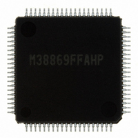
Manufacturer Part Number
M38869FFAHP#UU
Description
IC 740/3886 MCU FLASH 80LQFP
Manufacturer
Renesas Electronics America
Series
740/38000r
Datasheet
1.M38869FFAGPU0.pdf
(113 pages)
Specifications of M38869FFAHP#UU
Core Processor
740
Core Size
8-Bit
Speed
10MHz
Connectivity
I²C, SIO, UART/USART
Peripherals
PWM, WDT
Number Of I /o
64
Program Memory Size
60KB (60K x 8)
Program Memory Type
FLASH
Ram Size
2K x 8
Voltage - Supply (vcc/vdd)
4 V ~ 5.5 V
Data Converters
A/D 8x10b; D/A 2x8b
Oscillator Type
Internal
Operating Temperature
-20°C ~ 85°C
Package / Case
80-LQFP
Lead Free Status / RoHS Status
Lead free / RoHS Compliant
Eeprom Size
-
Available stocks
Company
Part Number
Manufacturer
Quantity
Price


[Data Bus Buffer Status Register 0, 1
(DBBSTS0, DBBSTS1)] 0029
The data bus buffer status register 0, 1 consist of eight bits.
Bits 0, 1, and 3 are read-only bits and indicate the condition of the
data bus buffer. Bits 2, 4, 5, 6, and 7 are user definable flags
which can be set by program, and can be read/written. This regis-
ter can be read from the host CPU when the A
only.
•Bit 0: Output buffer full flag OBF
•Bit 1: Input buffer full flag IBF
•Bit 3: A
[Input Data Bus Buffer Register 0, 1 (DBBIN0,
DBBIN1)] 0028
Data on the data bus is latched to DBBIN by writing request from
the host CPU. Data of DBBIN can be read from the data bus
buffer registers (address 0028
[Output Data Bus Buffer Register 0, 1
(DBBOUT0, DBBOUT1)] 0028
When writing data to the data bus buffer registers (address 0028
or 002B
output from the host CPU to the data bus by performing the read-
ing request when the A
38
When writing data to the output data bus buffer, these flags are
set to “1”. When reading the output data bus buffer from the host
CPU, these flags are cleared to “0”.
When writing data from the host CPU to the input data bus
buffer, these flags are set to “1”. When reading the input data
bus buffer from the slave CPU side, these flags are cleared to
“0”.
When writing data from the host CPU to the input data bus
buffer, the level of the A
16
0
) on SFR, data is set to DBBOUT. Data of DBBOUT is
flag A0
0
, A0
16
1
0
, 002B
pin is set to “L”.
0
pin is latched.
16
0
or 002B
16
, IBF
0
, OBF
1
16
16
16
1
) on SFR.
, 002C
, 002B
0
pin is set to “H”
16
16
16
SINGLE-CHIP 8-BIT CMOS MICROCOMPUTER
MITSUBISHI MICROCOMPUTERS
3886 Group
Related parts for M38869FFAHP#UU
Image
Part Number
Description
Manufacturer
Datasheet
Request
R

Part Number:
Description:
KIT STARTER FOR M16C/29
Manufacturer:
Renesas Electronics America
Datasheet:

Part Number:
Description:
KIT STARTER FOR R8C/2D
Manufacturer:
Renesas Electronics America
Datasheet:

Part Number:
Description:
R0K33062P STARTER KIT
Manufacturer:
Renesas Electronics America
Datasheet:

Part Number:
Description:
KIT STARTER FOR R8C/23 E8A
Manufacturer:
Renesas Electronics America
Datasheet:

Part Number:
Description:
KIT STARTER FOR R8C/25
Manufacturer:
Renesas Electronics America
Datasheet:

Part Number:
Description:
KIT STARTER H8S2456 SHARPE DSPLY
Manufacturer:
Renesas Electronics America
Datasheet:

Part Number:
Description:
KIT STARTER FOR R8C38C
Manufacturer:
Renesas Electronics America
Datasheet:

Part Number:
Description:
KIT STARTER FOR R8C35C
Manufacturer:
Renesas Electronics America
Datasheet:

Part Number:
Description:
KIT STARTER FOR R8CL3AC+LCD APPS
Manufacturer:
Renesas Electronics America
Datasheet:
Part Number:
Description:
KIT STARTER FOR RX610
Manufacturer:
Renesas Electronics America
Datasheet:

Part Number:
Description:
KIT STARTER FOR R32C/118
Manufacturer:
Renesas Electronics America
Datasheet:

Part Number:
Description:
KIT DEV RSK-R8C/26-29
Manufacturer:
Renesas Electronics America
Datasheet:

Part Number:
Description:
KIT STARTER FOR SH7124
Manufacturer:
Renesas Electronics America
Datasheet:

Part Number:
Description:
KIT STARTER FOR H8SX/1622
Manufacturer:
Renesas Electronics America
Datasheet:

Part Number:
Description:
KIT DEV FOR SH7203
Manufacturer:
Renesas Electronics America
Datasheet: