M30622F8PGP#U7C Renesas Electronics America, M30622F8PGP#U7C Datasheet - Page 279
M30622F8PGP#U7C
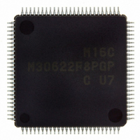
Manufacturer Part Number
M30622F8PGP#U7C
Description
IC M16C MCU FLASH 64K 100LQFP
Manufacturer
Renesas Electronics America
Series
M16C™ M16C/60r
Datasheets
1.QSK-62P_PLUS.pdf
(103 pages)
2.M30622SAFPU5.pdf
(308 pages)
3.M30620SPGPU3C.pdf
(423 pages)
Specifications of M30622F8PGP#U7C
Core Processor
M16C/60
Core Size
16-Bit
Speed
24MHz
Connectivity
I²C, IEBus, UART/USART
Peripherals
DMA, WDT
Number Of I /o
85
Program Memory Size
64KB (64K x 8)
Program Memory Type
FLASH
Ram Size
4K x 8
Voltage - Supply (vcc/vdd)
2.7 V ~ 5.5 V
Data Converters
A/D 26x10b; D/A 2x8b
Oscillator Type
Internal
Operating Temperature
-40°C ~ 85°C
Package / Case
100-LQFP
For Use With
867-1000 - KIT QUICK START RENESAS 62PM3062PT3-CPE-3 - EMULATOR COMPACT M16C/62P/30P
Lead Free Status / RoHS Status
Lead free / RoHS Compliant
Eeprom Size
-
Available stocks
Company
Part Number
Manufacturer
Quantity
Price

Part Number:
M30622F8PGP#U7CM30622F8PGP#D3C
Manufacturer:
Renesas Electronics America
Quantity:
10 000
Part Number:
M30622F8PGP#U7CM30622F8PGP#D5C
Manufacturer:
Renesas Electronics America
Quantity:
10 000


M16C/62P Group (M16C/62P, M16C/62PT)
Rev.2.41
REJ09B0185-0241
Figure 21.7
Port Pi Direction Register (i=0 to 7 and 9 to 13)
Port P8 Direction Register
b7 b6 b5 b4 b3 b2 b1 b0
NOTES :
b7 b6 b5 b4
1.
2.
3. To use ports P11 to P14, set the PU37 bit in the PUR3 register to “1” (enable).
Make sure the PD9 register is w ritten to by the next instruction after setting the PRC2 bit in the PRCR register to “1”
(w rite enabled).
During memory extension and microprocessor modes, the PDi register for the pins functioning as bus control pins (A0
to A19, D0 to D15, CS0
Jan 10, 2006
b3 b2 b1 b0
PDi Registers
Bit Symbol
Bit Symbol
PD0 to PD3
PD4 to PD7
PD9 to PD12
PD13
PD8_0
PD8_1
PD8_2
PD8_3
PD8_4
PD8_6
PD8_7
PDi_0
PDi_1
PDi_2
PDi_3
PDi_4
PDi_5
PDi_6
PDi_7
_____
(b5)
—
Page 262 of 390
Symbol
Symbol
to CS3
PD8
_____
Port Pi_0 Direction Bit
Port Pi_1 Direction Bit
Port Pi_2 Direction Bit
Port Pi_3 Direction Bit
Port Pi_4 Direction Bit
Port Pi_5 Direction Bit
Port Pi_6 Direction Bit
Port Pi_7 Direction Bit
Port P8_0 Direction Bit
Port P8_1 Direction Bit
Port P8_2 Direction Bit
Port P8_3 Direction Bit
Port P8_4 Direction Bit
Nothing is assigned. When w rite, set to “0”.
When read, its content is indeterminate.
Port P8_6 Direction Bit
Port P8_7 Direction Bit
, RD
___
, WRL
______
/WR
___
03E2h, 03E3h, 03E6h, 03E7h
03EAh, 03EBh, 03EEh, 03EFh
03F3h, 03F6h, 03F73h, 03FAh
03FBh
, WRH
Bit Name
Bit Name
______
(1, 2, 3)
/BHE
_____
Address
, ALE, RDY
Address
03F2h
_____
, HOLD
_______
0 : Input mode
1 : Output mode
0 : Input mode
1 : Output mode
0 : Input mode
1 : Output mode
(Functions as an input port)
(Functions as an output port)
(i = 0 to 7 and 9 to 13)
(Functions as an input port)
(Functions as an output port)
(Functions as an input port)
(Functions as an output port)
, HLDA
_______
and BCLK) cannot be modified.
Function
Function
21. Programmable I/O Ports
After Reset
After Reset
00X00000b
00h
00h
00h
00h
RW
RW
RW
RW
RW
RW
RW
RW
RW
RW
RW
RW
RW
RW
RW
RW
RW
—
Related parts for M30622F8PGP#U7C
Image
Part Number
Description
Manufacturer
Datasheet
Request
R

Part Number:
Description:
SINGLE-CHIP 16-BIT CMOS MICROCOMPUTER
Manufacturer:
Mitsubishi
Datasheet:

Part Number:
Description:
KIT STARTER FOR M16C/29
Manufacturer:
Renesas Electronics America
Datasheet:

Part Number:
Description:
KIT STARTER FOR R8C/2D
Manufacturer:
Renesas Electronics America
Datasheet:

Part Number:
Description:
R0K33062P STARTER KIT
Manufacturer:
Renesas Electronics America
Datasheet:

Part Number:
Description:
KIT STARTER FOR R8C/23 E8A
Manufacturer:
Renesas Electronics America
Datasheet:

Part Number:
Description:
KIT STARTER FOR R8C/25
Manufacturer:
Renesas Electronics America
Datasheet:

Part Number:
Description:
KIT STARTER H8S2456 SHARPE DSPLY
Manufacturer:
Renesas Electronics America
Datasheet:

Part Number:
Description:
KIT STARTER FOR R8C38C
Manufacturer:
Renesas Electronics America
Datasheet:

Part Number:
Description:
KIT STARTER FOR R8C35C
Manufacturer:
Renesas Electronics America
Datasheet:

Part Number:
Description:
KIT STARTER FOR R8CL3AC+LCD APPS
Manufacturer:
Renesas Electronics America
Datasheet:
Part Number:
Description:
KIT STARTER FOR RX610
Manufacturer:
Renesas Electronics America
Datasheet:

Part Number:
Description:
KIT STARTER FOR R32C/118
Manufacturer:
Renesas Electronics America
Datasheet:

Part Number:
Description:
KIT DEV RSK-R8C/26-29
Manufacturer:
Renesas Electronics America
Datasheet:

Part Number:
Description:
KIT STARTER FOR SH7124
Manufacturer:
Renesas Electronics America
Datasheet:

Part Number:
Description:
KIT STARTER FOR H8SX/1622
Manufacturer:
Renesas Electronics America
Datasheet: