MC908LJ24CPBE Freescale Semiconductor, MC908LJ24CPBE Datasheet - Page 213
MC908LJ24CPBE
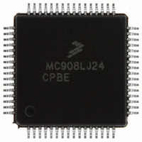
Manufacturer Part Number
MC908LJ24CPBE
Description
IC MCU 24K FLASH 8MHZ SPI 64LQFP
Manufacturer
Freescale Semiconductor
Series
HC08r
Datasheet
1.MC908LK24CFUE.pdf
(464 pages)
Specifications of MC908LJ24CPBE
Core Processor
HC08
Core Size
8-Bit
Speed
8MHz
Connectivity
I²C, IRSCI, SPI
Peripherals
LCD, LVD, POR, PWM
Number Of I /o
40
Program Memory Size
24KB (24K x 8)
Program Memory Type
FLASH
Ram Size
768 x 8
Voltage - Supply (vcc/vdd)
3 V ~ 5.5 V
Data Converters
A/D 6x10b
Oscillator Type
Internal
Operating Temperature
-40°C ~ 85°C
Package / Case
64-LQFP
Processor Series
HC08LJ
Core
HC08
Data Bus Width
8 bit
Data Ram Size
768 B
Interface Type
SCI/SPI
Maximum Clock Frequency
8 MHz
Number Of Programmable I/os
48
Number Of Timers
4
Operating Supply Voltage
3.3 V, 5 V
Maximum Operating Temperature
+ 85 C
Mounting Style
SMD/SMT
Development Tools By Supplier
FSICEBASE, M68EML08LJLKE, ZK-HC08LX-A, M68CBL05CE
Minimum Operating Temperature
- 40 C
On-chip Adc
6-ch x 10-bit
Controller Family/series
HC08
No. Of I/o's
40
Ram Memory Size
768Byte
Cpu Speed
8MHz
No. Of Timers
2
Embedded Interface Type
I2C, SCI, SPI
Rohs Compliant
Yes
Lead Free Status / RoHS Status
Lead free / RoHS Compliant
Eeprom Size
-
Lead Free Status / Rohs Status
Lead free / RoHS Compliant
Available stocks
Company
Part Number
Manufacturer
Quantity
Price
Company:

Part Number:
MC908LJ24CPBE
Manufacturer:
Freescale Semiconductor
Quantity:
10 000
Company:
Part Number:
MC908LJ24CPBER
Manufacturer:
Freescale Semiconductor
Quantity:
10 000


MC68HC908LJ24/LK24 — Rev. 2.1
Freescale Semiconductor
CHxF — Channel x Flag Bit
CHxIE — Channel x Interrupt Enable Bit
MSxB — Mode Select Bit B
MSxA — Mode Select Bit A
When channel x is an input capture channel, this read/write bit is set
when an active edge occurs on the channel x pin. When channel x is
an output compare channel, CHxF is set when the value in the TIM
counter registers matches the value in the TIM channel x registers.
When TIM CPU interrupt requests are enabled (CHxIE = 1), clear
CHxF by reading TIM channel x status and control register with CHxF
set and then writing a logic 0 to CHxF. If another interrupt request
occurs before the clearing sequence is complete, then writing logic 0
to CHxF has no effect. Therefore, an interrupt request cannot be lost
due to inadvertent clearing of CHxF.
Reset clears the CHxF bit. Writing a logic 1 to CHxF has no effect.
This read/write bit enables TIM CPU interrupt service requests on
channel x.
Reset clears the CHxIE bit.
This read/write bit selects buffered output compare/PWM operation.
MSxB exists only in the TIM1 channel 0 and TIM2 channel 0 status
and control registers.
Setting MS0B disables the channel 1 status and control register and
reverts TCH1 to general-purpose I/O.
Reset clears the MSxB bit.
When ELSxB:ELSxA ≠ 0:0, this read/write bit selects either input
capture operation or unbuffered output compare/PWM operation.
See
1 = Input capture or output compare on channel x
0 = No input capture or output compare on channel x
1 = Channel x CPU interrupt requests enabled
0 = Channel x CPU interrupt requests disabled
1 = Buffered output compare/PWM operation enabled
0 = Buffered output compare/PWM operation disabled
1 = Unbuffered output compare/PWM operation
0 = Input capture operation
Table
Timer Interface Module (TIM)
11-3.
Timer Interface Module (TIM)
I/O Registers
Data Sheet
213
Related parts for MC908LJ24CPBE
Image
Part Number
Description
Manufacturer
Datasheet
Request
R

Part Number:
Description:
Manufacturer:
Freescale Semiconductor, Inc
Datasheet:
Part Number:
Description:
Manufacturer:
Freescale Semiconductor, Inc
Datasheet:
Part Number:
Description:
Manufacturer:
Freescale Semiconductor, Inc
Datasheet:
Part Number:
Description:
Manufacturer:
Freescale Semiconductor, Inc
Datasheet:
Part Number:
Description:
Manufacturer:
Freescale Semiconductor, Inc
Datasheet:
Part Number:
Description:
Manufacturer:
Freescale Semiconductor, Inc
Datasheet:
Part Number:
Description:
Manufacturer:
Freescale Semiconductor, Inc
Datasheet:
Part Number:
Description:
Manufacturer:
Freescale Semiconductor, Inc
Datasheet:
Part Number:
Description:
Manufacturer:
Freescale Semiconductor, Inc
Datasheet:
Part Number:
Description:
Manufacturer:
Freescale Semiconductor, Inc
Datasheet:
Part Number:
Description:
Manufacturer:
Freescale Semiconductor, Inc
Datasheet:
Part Number:
Description:
Manufacturer:
Freescale Semiconductor, Inc
Datasheet:
Part Number:
Description:
Manufacturer:
Freescale Semiconductor, Inc
Datasheet:
Part Number:
Description:
Manufacturer:
Freescale Semiconductor, Inc
Datasheet:
Part Number:
Description:
Manufacturer:
Freescale Semiconductor, Inc
Datasheet: