Z8F022ASJ020SC Zilog, Z8F022ASJ020SC Datasheet - Page 8
Z8F022ASJ020SC
Manufacturer Part Number
Z8F022ASJ020SC
Description
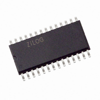
IC ENCORE XP MCU FLASH 2K 28SOIC
Manufacturer
Zilog
Series
Encore!® XP®r
Specifications of Z8F022ASJ020SC
Core Processor
Z8
Core Size
8-Bit
Speed
20MHz
Connectivity
IrDA, UART/USART
Peripherals
Brown-out Detect/Reset, LED, LVD, POR, PWM, Temp Sensor, WDT
Number Of I /o
23
Program Memory Size
2KB (2K x 8)
Program Memory Type
FLASH
Eeprom Size
64 x 8
Ram Size
512 x 8
Voltage - Supply (vcc/vdd)
2.7 V ~ 3.6 V
Data Converters
A/D 8x10b
Oscillator Type
Internal
Operating Temperature
0°C ~ 70°C
Package / Case
28-SOIC (7.5mm Width)
Lead Free Status / RoHS Status
Contains lead / RoHS non-compliant
Other names
269-3355
Available stocks
Company
Part Number
Manufacturer
Quantity
Price
Company:

Part Number:
Z8F022ASJ020SC
Manufacturer:
Zilog
Quantity:
372


Table 4. Z8 Encore! XP
UP006912-0308
Sl
No. Summary
9
10
11
12
13
14
15
WDT Default
Timeout Period
longer than
specified.
IPO current
consumption higher
than typically
specified.
Open Drain Output
Control only on Port
A.
ADC Internal
Reference Voltage
Error.
STOP mode current
out of specification.
Unstable
Comparator Output.
External Vref is not
available on 20-pin
parts.
0426 and Before 0440 (Continued)
®
Description
In the product specification the default timeout period is 100 ms. However, for
this version of silicon, the default is equal to the maximum timeout value.
Workaround
Manually set the WDT timeout to the desired value.
When the IPO is enabled, the product specification gives a typical current
consumption of 300 µA. The consumption for these date codes is typically 1.5
mA.
Workaround
None.
Open drain output configuration set by Port A-D Output Control sub registers
is possible only for Port A pins. It is not possible to configure Port B, C, D pins
for open drain output.
Workaround
None. Use Port A pins for open drain output.
Internal Reference Voltage (Vref) set by REFSEL field in the ADC Control
Register was not set optimally, reporting 1.91 V for a specified 2.0 V setting.
Workaround
None. External Vref sourced ADC measurements are not affected by this
errata.
Measured STOP mode current with LPO ON is 50 µA typical versus the
specified 10 µA. STOP mode current with all peripherals OFF is 4 µA typical
versus the specified 2 µA.
Workaround
None.
Internal reference voltage level set by the REFLVL field in the Comparator
Control Register causes an unstable comparator output, worsening as the
internal reference voltage increases.
Workaround
None.
For 20-pin devices, external Vref is not an option on pin PC2.
Workaround
None.
F082A Series Errata (20- and 28-pin Devices) with Date Codes
Errata for Z8 Encore! XP
®
F082A Series
Page 8 of 14
Related parts for Z8F022ASJ020SC
Image
Part Number
Description
Manufacturer
Datasheet
Request
R

Part Number:
Description:
Communication Controllers, ZILOG INTELLIGENT PERIPHERAL CONTROLLER (ZIP)
Manufacturer:
Zilog, Inc.
Datasheet:

Part Number:
Description:
KIT DEV FOR Z8 ENCORE 16K TO 64K
Manufacturer:
Zilog
Datasheet:

Part Number:
Description:
KIT DEV Z8 ENCORE XP 28-PIN
Manufacturer:
Zilog
Datasheet:

Part Number:
Description:
DEV KIT FOR Z8 ENCORE 8K/4K
Manufacturer:
Zilog
Datasheet:

Part Number:
Description:
KIT DEV Z8 ENCORE XP 28-PIN
Manufacturer:
Zilog
Datasheet:

Part Number:
Description:
DEV KIT FOR Z8 ENCORE 4K TO 8K
Manufacturer:
Zilog
Datasheet:
Part Number:
Description:
CMOS Z8 microcontroller. ROM 16 Kbytes, RAM 256 bytes, speed 16 MHz, 32 lines I/O, 3.0V to 5.5V
Manufacturer:
Zilog, Inc.
Datasheet:
Part Number:
Description:
Low-cost microcontroller. 512 bytes ROM, 61 bytes RAM, 8 MHz
Manufacturer:
Zilog, Inc.
Datasheet:
Part Number:
Description:
Z8 4K OTP Microcontroller
Manufacturer:
Zilog, Inc.
Datasheet:
Part Number:
Description:
CMOS SUPER8 ROMLESS MCU
Manufacturer:
Zilog, Inc.
Datasheet:
Part Number:
Description:
SL1866 CMOSZ8 OTP Microcontroller
Manufacturer:
Zilog, Inc.
Datasheet:
Part Number:
Description:
SL1866 CMOSZ8 OTP Microcontroller
Manufacturer:
Zilog, Inc.
Datasheet:
Part Number:
Description:
OTP (KB) = 1, RAM = 125, Speed = 12, I/O = 14, 8-bit Timers = 2, Comm Interfaces Other Features = Por, LV Protect, Voltage = 4.5-5.5V
Manufacturer:
Zilog, Inc.
Datasheet:
Part Number:
Description:
Manufacturer:
Zilog, Inc.
Datasheet: