PIC32MX575F512H-80I/MR Microchip Technology, PIC32MX575F512H-80I/MR Datasheet - Page 59
PIC32MX575F512H-80I/MR
Manufacturer Part Number
PIC32MX575F512H-80I/MR
Description
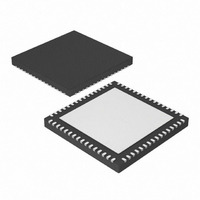
IC MCU 32BIT 512KB FLASH 64QFN
Manufacturer
Microchip Technology
Series
PIC® 32MXr
Datasheets
1.PIC32MX320F032H-40IPT.pdf
(66 pages)
2.PIC32MX575F256H-80IMR.pdf
(2 pages)
3.PIC32MX575F256H-80IMR.pdf
(254 pages)
4.PIC32MX575F256H-80IMR.pdf
(14 pages)
5.PIC32MX575F256H-80IPT.pdf
(240 pages)
Specifications of PIC32MX575F512H-80I/MR
Core Size
32-Bit
Program Memory Size
512KB (512K x 8)
Core Processor
MIPS32® M4K™
Speed
80MHz
Connectivity
CAN, I²C, SPI, UART/USART, USB OTG
Peripherals
Brown-out Detect/Reset, DMA, POR, PWM, WDT
Number Of I /o
53
Program Memory Type
FLASH
Ram Size
64K x 8
Voltage - Supply (vcc/vdd)
2.3 V ~ 3.6 V
Data Converters
A/D 16x10b
Oscillator Type
Internal
Operating Temperature
-40°C ~ 85°C
Package / Case
64-VFQFN, Exposed Pad
Controller Family/series
PIC32
Ram Memory Size
64KB
Cpu Speed
80MHz
No. Of Timers
5
Interface
CAN, I2C, SPI, UART, USB
No. Of Pwm Channels
5
Embedded Interface Type
CAN, I2C, SPI, UART, USB
Rohs Compliant
Yes
Processor Series
PIC32MX5xx
Core
MIPS
3rd Party Development Tools
52713-733, 52714-737
Development Tools By Supplier
PG164130, DV164035, DV244005
Lead Free Status / RoHS Status
Lead free / RoHS Compliant
Eeprom Size
-
Lead Free Status / Rohs Status
Details


20.0
TABLE 20-1:
© 2010 Microchip Technology Inc.
Standard Operating Conditions
Operating Temperature: 0ºC to +70ºC. Programming at +25ºC is recommended.
D111
D112
D113
D031
D041
D080
D090
D012
D013
P1
P1A
P1B
P2
P3
P4
P4A
P5
P6
P7
P8
P9A
P9B
P10
P11
P12
P13
P14
P15
P16
Note 1:
Param
No.
2:
AC/DC CHARACTERISTICS
AND TIMING REQUIREMENTS
V
I
I
V
V
V
V
C
C
T
T
T
T
T
T
T
T
T
T
T
T
T
T
T
T
T
T
T
T
Symbol
PP
DDP
PGC
PGCL
PGCH
SET
HLD
DLY
DLY
DLY
SET
HLD
DLY
DLY
DLY
DLY
DLY
DLY
DLY
R
VALID
DLY
DD
IL
IH
OL
OH
IO
F
V
“Power Requirements” for more information.
V
±0.3V of V
DDCORE
DD
1
1
1
2
2
3
4
5
6
7
8
9
8
1
2
A
must also be supplied to the AV
AC/DC CHARACTERISTICS AND TIMING REQUIREMENTS
Supply Voltage During Programming
Programming Current on MCLR
Supply Current During Programming
Input Low Voltage
Input High Voltage
Output Low Voltage
Output High Voltage
Capacitive Loading on I/O pin (PGDx)
Filter Capacitor Value on V
Serial Clock (PGCx) Period
Serial Clock (PGCx) Low Time
Serial Clock (PGCx) High Time
Input Data Setup Time to Serial Clock ↓
Input Data Hold Time from PGCx ↓
Delay between 4-bit Command and
Command Operand
Delay between 4-bit Command Operand
and Next 4-bit Command
Delay between Last PGCx ↓ of Com-
mand Byte to First PGCx ↑ of Read of
Data Word
V
Input Data Hold Time from MCLR ↑
Delay between Last PGCx ↓ of Com-
mand Byte to PGDx ↑ by the PE
PE Command
Processing Time
Delay between PGDx ↓ by the PE to
PGDx Released by the PE
PGCx Low Time After Programming
Chip Erase Time
Page Erase Time
Row Programming Time
MCLR Rise Time to Enter ICSP™ mode
Data Out Valid from PGCx ↑
Delay between Last PGCx ↓ and MCLR
↓
DD
must be supplied to the V
DD
↑ Setup Time to MCLR ↑
and V
SS
Characteristic
, respectively.
CAP
DDCORE
DD
pins during programming. AV
/V
CAP
pin if the on-chip voltage regulator is disabled. See 4.3
0.8 V
Min.
3.0V
V
100
100
500
400
1.4
—
—
40
40
15
15
40
40
20
20
40
15
80
20
10
—
—
—
1
2
0
SS
DD
0.2 V
Max.
3.60
V
0.4
1.0
40
50
10
—
—
—
—
—
—
—
—
—
—
—
—
—
—
—
—
—
—
—
—
5
DD
DD
DD
and AV
Units
mA
μA
ms
ms
ms
pF
μF
ns
ns
ns
ns
ns
ns
ns
ns
ns
ns
μs
μs
μs
ns
μs
ns
V
V
V
V
V
s
SS
Normal programming
I
I
To meet AC specifications
Required for controller core
OL
OH
should always be within
PIC32MX
= 8.5 mA @ 3.6V
= -3.0 mA @ 3.6V
Conditions
DS61145G-page 59
—
—
—
—
—
—
—
—
—
—
—
—
—
—
—
—
—
—
—
—
—
—
—
—
(1,2)
Related parts for PIC32MX575F512H-80I/MR
Image
Part Number
Description
Manufacturer
Datasheet
Request
R

Part Number:
Description:
Manufacturer:
Microchip Technology Inc.
Datasheet:
Part Number:
Description:
Manufacturer:
Microchip Technology Inc.
Datasheet:
Part Number:
Description:
Manufacturer:
Microchip Technology Inc.
Datasheet:
Part Number:
Description:
Manufacturer:
Microchip Technology Inc.
Datasheet:
Part Number:
Description:
Manufacturer:
Microchip Technology Inc.
Datasheet:
Part Number:
Description:
Manufacturer:
Microchip Technology Inc.
Datasheet:
Part Number:
Description:
Manufacturer:
Microchip Technology Inc.
Datasheet:
Part Number:
Description:
Manufacturer:
Microchip Technology Inc.
Datasheet: