PIC18F14K50-I/P Microchip Technology, PIC18F14K50-I/P Datasheet - Page 242
PIC18F14K50-I/P
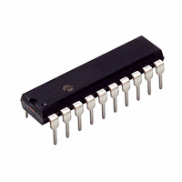
Manufacturer Part Number
PIC18F14K50-I/P
Description
IC PIC MCU FLASH 8KX16 20-PDIP
Manufacturer
Microchip Technology
Series
PIC® XLP™ 18Fr
Datasheets
1.PIC18F13K50-ISS.pdf
(420 pages)
2.PIC18F13K50-ISS.pdf
(10 pages)
3.PIC18F13K50-ISS.pdf
(2 pages)
4.PIC18F14K50-ISS.pdf
(4 pages)
5.PIC18F14K50-IP.pdf
(422 pages)
Specifications of PIC18F14K50-I/P
Program Memory Type
FLASH
Program Memory Size
16KB (8K x 16)
Package / Case
20-DIP (0.300", 7.62mm)
Core Processor
PIC
Core Size
8-Bit
Speed
48MHz
Connectivity
I²C, SPI, UART/USART, USB
Peripherals
Brown-out Detect/Reset, POR, PWM, WDT
Number Of I /o
14
Eeprom Size
256 x 8
Ram Size
768 x 8
Voltage - Supply (vcc/vdd)
1.8 V ~ 5.5 V
Data Converters
A/D 11x10b
Oscillator Type
Internal
Operating Temperature
-40°C ~ 85°C
Processor Series
PIC18F
Core
PIC
Data Bus Width
8 bit
Data Ram Size
768 B
Interface Type
EUSART/I2C/MSSP/SPI/USB
Maximum Clock Frequency
48 MHz
Number Of Programmable I/os
15
Number Of Timers
4
Maximum Operating Temperature
+ 85 C
Mounting Style
Through Hole
3rd Party Development Tools
52715-96, 52716-328, 52717-734, 52712-325, EWPIC18
Development Tools By Supplier
PG164130, DV164035, DV244005, DV164005
Minimum Operating Temperature
- 40 C
On-chip Adc
11-ch x 10-bit
Package
20PDIP
Device Core
PIC
Family Name
PIC18
Maximum Speed
48 MHz
Operating Supply Voltage
3.3|5 V
Lead Free Status / RoHS Status
Lead free / RoHS Compliant
For Use With
AC244023 - PROC EXTENS PAK PIC18F1XK50DV164126 - KIT DEVELOPMENT USB W/PICKIT 2DM164127 - KIT DEVELOPMENT USB 18F14/13K50AC164112 - VOLTAGE LIMITER MPLAB ICD2 VPP
Lead Free Status / Rohs Status
Lead free / RoHS Compliant


PIC18F/LF1XK50
TABLE 20-2:
REGISTER 20-1:
DS41350E-page 242
bit 7
Legend:
R = Readable bit
-n = Value at POR
bit 7
bit 6-4
bit 3
bit 2
bit 1
bit 0
Note 1:
SRCLK
SRLEN
R/W-0
111
110
101
100
011
010
001
000
Changing the SRCLK bits while the SR latch is enabled may cause false triggers to the set and Reset
inputs of the latch.
SRLEN: SR Latch Enable bit
1 = SR latch is enabled
0 = SR latch is disabled
SRCLK<2:0>
000 = 1/4 Peripheral cycle clock
001 = 1/8 Peripheral cycle clock
010 = 1/16 Peripheral cycle clock
011 = 1/32 Peripheral cycle clock
100 = 1/64 Peripheral cycle clock
101 = 1/128 Peripheral cycle clock
110 = 1/256 Peripheral cycle clock
111 = 1/512 Peripheral cycle clock
SRQEN: SR Latch Q Output Enable bit
If SRNQEN = 0
1 = Q is present on the RC4 pin
0 = Q is internal only
SRNQEN: SR Latch Q Output Enable bit
1 = Q is present on the RC4 pin
0 = Q is internal only
SRPS: Pulse Set Input of the SR Latch
1 = Pulse input
0 = Always reads back ‘0’
SRPR: Pulse Reset Input of the SR Latch
1 = Pulse input
0 = Always reads back ‘0’
Divider
SRCLK FREQUENCY TABLE
512
256
128
SRCLK2
64
32
16
8
4
R/W-0
SRCON0: SR LATCH CONTROL REGISTER
F
(1)
OSC
W = Writable bit
‘1’ = Bit is set
: SR Latch Clock divider bits
SRCLK1
25.6 s
12.8 s
6.4 s
3.2 s
1.6 s
0.8 s
0.4 s
0.2 s
R/W-0
= 20 MHz
(1)
SRCLK0
F
R/W-0
OSC
Preliminary
0.25 s
0.5 s
32 s
16 s
8 s
4 s
2 s
1 s
= 16 MHz
U = Unimplemented
‘0’ = Bit is cleared
SRQEN
R/W-0
F
OSC
0.5 s
64 s
32 s
16 s
8 s
4 s
2 s
1 s
= 8 MHz F
SRNQEN
R/W-0
OSC
128 s
2010 Microchip Technology Inc.
64 s
32 s
16 s
8 s
4 s
2 s
1 s
= 4 MHz
C = Clearable only bit
x = Bit is unknown
R/W-0
SRPS
F
OSC
512 s
256 s
128 s
64 s
32 s
16 s
8 s
4 s
R/W-0
SRPR
= 1 MHz
bit 0
Related parts for PIC18F14K50-I/P
Image
Part Number
Description
Manufacturer
Datasheet
Request
R

Part Number:
Description:
20-Pin USB Flash Microcontrollers
Manufacturer:
MICROCHIP [Microchip Technology]
Datasheet:

Part Number:
Description:
PIC18F With 128-segment LCD Driver And 12-bit ADC, 8KB Flash, 768B RAM, CCP, MSS
Manufacturer:
Microchip Technology
Datasheet:
Part Number:
Description:
PIC18F With 128-segment LCD Driver And 12-bit ADC, 16KB Flash, 768B RAM, CCP, MS
Manufacturer:
Microchip Technology
Datasheet:

Part Number:
Description:
PIC18F With 192-segment LCD Driver And 12-bit ADC, 8KB Flash, 768B RAM, CCP, MSS
Manufacturer:
Microchip Technology
Datasheet:
Part Number:
Description:
PIC18F With 192-segment LCD Driver And 12-bit ADC, 16KB Flash, 768B RAM, CCP, MS
Manufacturer:
Microchip Technology
Datasheet:

Part Number:
Description:
Microcontrollers (MCU) 48KB 3328 RAM 52 I/O
Manufacturer:
Microchip Technology
Datasheet:
Part Number:
Description:
Microcontrollers (MCU) 64KB 3328 RAM 52 I/O
Manufacturer:
Microchip Technology
Datasheet:

Part Number:
Description:
32kB Flash, 2kB RAM, 1kB EE, NanoWatt XLP, LCD 64 QFN 9x9x0.9mm T/R
Manufacturer:
Microchip Technology
Datasheet:

Part Number:
Description:
32kB Flash, 2kB RAM, 1kB EE, NanoWatt XLP, LCD 64 TQFP 10x10x1mm T/R
Manufacturer:
Microchip Technology
Datasheet:

Part Number:
Description:
128kB Flash, 4kB RAM, 1kB EE, 16MIPS, NanoWatt XLP, LCD, 5V 80 TQFP 12x12x1mm T/
Manufacturer:
Microchip Technology
Datasheet:
Part Number:
Description:
32kB Flash, 2kB RAM, 1kB EE, NanoWatt XLP, LCD 64 QFN 9x9x0.9mm TUBE
Manufacturer:
Microchip Technology
Datasheet:
Part Number:
Description:
32kB Flash, 2kB RAM, 1kB EE, NanoWatt XLP, LCD 64 TQFP 10x10x1mm TRAY
Manufacturer:
Microchip Technology
Part Number:
Description:
128kB Flash, 4kB RAM, 1kB EE, 16MIPS, NanoWatt XLP, LCD, 5V 80 TQFP 12x12x1mm TR
Manufacturer:
Microchip Technology
