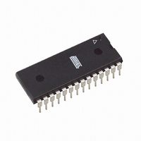
ATTINY88-PU Atmel, ATTINY88-PU Datasheet - Page 54

ATTINY88-PU
Manufacturer Part Number
ATTINY88-PU
Description
MCU AVR 8K ISP FLASH 1.8V 28-DIP
Manufacturer
Atmel
Series
AVR® ATtinyr
Specifications of ATTINY88-PU
Core Processor
AVR
Core Size
8-Bit
Speed
12MHz
Connectivity
I²C, SPI
Peripherals
Brown-out Detect/Reset, POR, WDT
Number Of I /o
24
Program Memory Size
8KB (4K x 16)
Program Memory Type
FLASH
Eeprom Size
64 x 8
Ram Size
512 x 8
Voltage - Supply (vcc/vdd)
1.8 V ~ 5.5 V
Data Converters
A/D 6x10b
Oscillator Type
Internal
Operating Temperature
-40°C ~ 85°C
Package / Case
28-DIP (0.300", 7.62mm)
Processor Series
ATTINY8x
Core
AVR8
Data Bus Width
8 bit
Data Ram Size
512 B
Interface Type
2-Wire/I2S/SPI
Maximum Clock Frequency
12 MHz
Number Of Programmable I/os
24
Number Of Timers
2
Maximum Operating Temperature
+ 85 C
Mounting Style
Through Hole
3rd Party Development Tools
EWAVR, EWAVR-BL
Development Tools By Supplier
ATAVRDRAGON, ATSTK500, ATSTK600, ATAVRISP2, ATAVRONEKIT, ATQT600, ATAVRTS2080B
Minimum Operating Temperature
- 40 C
On-chip Adc
6-ch x 10-bit
For Use With
ATSTK600 - DEV KIT FOR AVR/AVR32ATAVRDRAGON - KIT DRAGON 32KB FLASH MEM AVR
Lead Free Status / RoHS Status
Lead free / RoHS Compliant
Available stocks
Company
Part Number
Manufacturer
Quantity
Price
Company:
Part Number:
ATTINY88-PU
Manufacturer:
Atmel
Quantity:
3 360
- Current page: 54 of 302
- Download datasheet (9Mb)
9.2.1
9.2.2
54
ATtiny48/88
Pin Change Interrupt Timing
Low Level Interrupt
means that these interrupts can be used for waking the part also from sleep modes other than
Idle mode.
The INT0 and INT1 interrupts can be triggered by a falling or rising edge, or a low level. This is
configured as described in
INT0 or INT1 interrupts are enabled and are configured as level triggered, the interrupts will trig-
ger as long as the corresponding pin is held low. Note that recognition of falling or rising edge
interrupts on INT0 or INT1 requires the presence of an I/O clock, described in
clkI/O” on page
An example of timing of a pin change interrupt is shown in
Figure 9-1.
Low level interrupts on INT0 and INT1 are detected asynchronously. This means that the inter-
rupt sources can be used for waking the part also from sleep modes other than Idle (the I/O
clock is halted in all sleep modes except Idle mode).
Note that if a level triggered interrupt is used for wake-up from Power-down, the required level
must be held long enough for the MCU to complete the wake-up to trigger the level interrupt. If
the level disappears before the end of the Start-up Time, the MCU will still wake up, but no inter-
pcint_setflag
pcint_in_(0)
PCINT(0)
pcint_syn
pin_sync
pin_lat
PCINT(0)
PCIF
clk
clk
Timing of pin change interrupts
28.
LE
pin_lat
D
“EICRA – External Interrupt Control Register A” on page
Q
pin_sync
PCINT(0) in PCMSK(x)
pcint_in_(0)
0
x
clk
Figure
9-1.
pcint_syn
pcint_setflag
8008G–AVR–04/11
“I/O Clock –
55. When
PCIF
Related parts for ATTINY88-PU
Image
Part Number
Description
Manufacturer
Datasheet
Request
R

Part Number:
Description:
IC, MCU, 8BIT, 2K FLASH, 20SOIC
Manufacturer:
Atmel
Datasheet:

Part Number:
Description:
IC, MCU, 8BIT, 2K FLASH, 20PDIP
Manufacturer:
Atmel
Datasheet:

Part Number:
Description:
IC, MCU, 8BIT, 8K FLASH, 20PDIP
Manufacturer:
Atmel
Datasheet:

Part Number:
Description:
IC, MCU, 8BIT, 8K FLASH, 20SOIC
Manufacturer:
Atmel
Datasheet:

Part Number:
Description:
DEV KIT FOR AVR/AVR32
Manufacturer:
Atmel
Datasheet:

Part Number:
Description:
INTERVAL AND WIPE/WASH WIPER CONTROL IC WITH DELAY
Manufacturer:
ATMEL Corporation
Datasheet:

Part Number:
Description:
Low-Voltage Voice-Switched IC for Hands-Free Operation
Manufacturer:
ATMEL Corporation
Datasheet:

Part Number:
Description:
MONOLITHIC INTEGRATED FEATUREPHONE CIRCUIT
Manufacturer:
ATMEL Corporation
Datasheet:

Part Number:
Description:
AM-FM Receiver IC U4255BM-M
Manufacturer:
ATMEL Corporation
Datasheet:

Part Number:
Description:
Monolithic Integrated Feature Phone Circuit
Manufacturer:
ATMEL Corporation
Datasheet:

Part Number:
Description:
Multistandard Video-IF and Quasi Parallel Sound Processing
Manufacturer:
ATMEL Corporation
Datasheet:

Part Number:
Description:
High-performance EE PLD
Manufacturer:
ATMEL Corporation
Datasheet:


