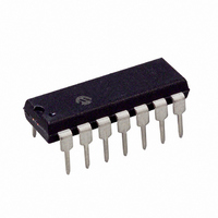
PIC16F506-I/P Microchip Technology, PIC16F506-I/P Datasheet - Page 4

PIC16F506-I/P
Manufacturer Part Number
PIC16F506-I/P
Description
IC PIC MCU FLASH 1KX14 14DIP
Manufacturer
Microchip Technology
Series
PIC® 16Fr
Datasheets
1.PIC12F510-ISN.pdf
(124 pages)
2.PIC16F506-ISL.pdf
(12 pages)
3.PIC16F506-ISL.pdf
(8 pages)
4.PIC16F506-ISL.pdf
(22 pages)
5.PIC16F506-IP.pdf
(114 pages)
Specifications of PIC16F506-I/P
Program Memory Type
FLASH
Program Memory Size
1.5KB (1K x 12)
Package / Case
14-DIP (0.300", 7.62mm)
Core Processor
PIC
Core Size
8-Bit
Speed
20MHz
Peripherals
POR, WDT
Number Of I /o
11
Ram Size
67 x 8
Voltage - Supply (vcc/vdd)
2 V ~ 5.5 V
Data Converters
A/D 4x8b
Oscillator Type
Internal
Operating Temperature
-40°C ~ 85°C
Processor Series
PIC16F
Core
PIC
Data Bus Width
8 bit
Data Ram Size
67 B
Maximum Clock Frequency
20 MHz
Number Of Programmable I/os
12
Number Of Timers
1
Maximum Operating Temperature
+ 85 C
Mounting Style
Through Hole
3rd Party Development Tools
52715-96, 52716-328, 52717-734
Development Tools By Supplier
PG164130, DV164035, DV244005, DV164005, PG164120, ICE2000
Minimum Operating Temperature
- 40 C
On-chip Adc
3-ch x 8-bit
Lead Free Status / RoHS Status
Lead free / RoHS Compliant
For Use With
AC162070 - HEADER INTRFC MPLAB ICD2 8/14P
Eeprom Size
-
Connectivity
-
Lead Free Status / Rohs Status
Lead free / RoHS Compliant
Available stocks
Company
Part Number
Manufacturer
Quantity
Price
Part Number:
PIC16F506-I/P
Manufacturer:
MICROCHIP/微芯
Quantity:
20 000
PIC16F506
3.0
3.1
The Program/Verify mode is entered by holding pins
ICSPCLK and ICSPDAT low while raising V
V
this mode, the user program memory and configuration
memory can be accessed and programmed in serial
fashion. Clock and data are Schmitt Trigger input in this
mode (see Figure 3-1).
The sequence that enters the device into the
Programming/Verify mode places all other logic into the
Reset state (the MCLR pin was initially at V
means that all I/O are in the Reset state (high-
impedance inputs).
3.1.1
The programming sequence loads a word, programs,
verifies and finally increments the PC.
Program/Verify mode entry will set the address to
0x7FF.
increment the PC. The available commands are shown
in Table 3-1.
FIGURE 3-1:
TABLE 3-1:
DS41258C-page 4
Load Data for Program Memory
Read Data from Program Memory
Increment Address
Begin Programming
End Programming
Bulk Erase Program Memory
IL
ICSPCLK
ICSPDAT
to V
V
V
DD
DD
PP
COMMANDS AND
ALGORITHMS
Program/Verify Mode
The
. Then raise V
PROGRAMMING
Increment
Command
COMMAND MAPPING FOR PIC16F506
T
PPDP
ENTERING HIGH
VOLTAGE PROGRAM/
VERIFY MODE
PP
Address
from V
T
HLD
0
IL
to V
command
IHH
DD
. Once in
pin from
IL
x
x
x
x
x
x
). This
will
x
x
x
x
x
x
Mapping (MSb … LSb)
0
0
0
1
1
1
3.1.2
The ICSPCLK pin is used for clock input and the
ICSPDAT pin is used for data input/output during serial
operation. To input a command, the clock pin is cycled
six times. Each command bit is latched on the falling
edge of the clock with the LSb of the command being
input first. The data must adhere to the setup (T
and hold (T
of the clock (see Table 6-1).
Commands that do not have data associated with them
are required to wait a minimum of T
from the falling edge of the last command clock to the
rising edge of the next command clock (see Table 6-1).
Commands that do have data associated with them
(Read and Load) are also required to wait T
between the command and the data segment
measured from the falling edge of the last command
clock to the rising edge of the first data clock. The data
segment, consisting of 16 clock cycles, can begin after
this delay.
The first and last clock pulses during the data segment
correspond to the Start and Stop bits, respectively.
Input data is a “don’t care” during the Start and Stop
cycles. The 14 clock pulses between the Start and Stop
cycles, clock the 14 bits of input/output data. Data is
transferred LSb first.
During Read commands, in which the data is output
from the PIC16F506, the ICSPDAT pin transitions from
the high-impedance input state to the low-impedance
output state at the rising edge of the second data clock
(first clock edge after the Start cycle). The ICSPDAT pin
returns to the high-impedance state at the rising edge
of the 16th data clock (first edge of the Stop cycle). See
Figure 3-3.
The commands that are available are described in
Table 3-1.
Note:
0
1
1
0
1
0
HLD
SERIAL PROGRAM/VERIFY
OPERATION
After every End Programming command,
a delay of T
1
0
1
0
1
0
1) times with respect to the falling edge
0
0
0
0
0
1
DIS
2010 Microchip Technology Inc.
must be delayed.
0, data (14), 0
0, data (14), 0
Externally Timed
Internally Timed
Data
DLY
2 measured
SET
DLY
1)
2


