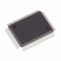
DS5002FPM-16+ Maxim Integrated Products, DS5002FPM-16+ Datasheet - Page 18

DS5002FPM-16+
Manufacturer Part Number
DS5002FPM-16+
Description
IC MPU SECURE 16MHZ 80-TQFP
Manufacturer
Maxim Integrated Products
Series
DS500xr
Datasheet
1.DS5002FPM-16.pdf
(25 pages)
Specifications of DS5002FPM-16+
Core Processor
8051
Core Size
8-Bit
Speed
16MHz
Connectivity
EBI/EMI, SIO, UART/USART
Peripherals
Power-Fail Reset, WDT
Number Of I /o
32
Program Memory Type
SRAM
Ram Size
128 x 8
Voltage - Supply (vcc/vdd)
4.5 V ~ 5.5 V
Oscillator Type
External
Operating Temperature
0°C ~ 70°C
Package / Case
80-MQFP, 80-PQFP
Processor Series
DS500x
Core
8051
Data Bus Width
8 bit
Data Ram Size
128 B
Maximum Clock Frequency
16 MHz
Number Of Programmable I/os
32
Number Of Timers
2
Operating Supply Voltage
3.85 V to 5.5 V
Maximum Operating Temperature
+ 70 C
Mounting Style
SMD/SMT
3rd Party Development Tools
PK51, CA51, A51, ULINK2
Minimum Operating Temperature
0 C
Program Memory Size
32 KB, 64 KB, 128 KB
Interface Type
UART
Package
80MQFP
Device Core
8051
Family Name
DS500x
Maximum Speed
16 MHz
Lead Free Status / RoHS Status
Lead free / RoHS Compliant
Eeprom Size
-
Program Memory Size
-
Data Converters
-
Lead Free Status / Rohs Status
Lead free / RoHS Compliant
DS5002FP Secure Microprocessor Chip
observe such relationships. Although it is very unlikely that an application program could be deciphered by
observing vector address relationships, the vector RAM eliminates this possibility. Note that the dummy accesses
mentioned above are conducted while fetching from vector RAM.
The vector RAM is automatically loaded with the user’s reset and interrupt vectors during bootstrap loading.
SECURITY LOCK
Once the application program has been loaded into the DS5002FP’s NV RAM, the security lock can be enabled by
issuing the “Z” command in the bootstrap loader. While the security lock is set, no further access to program/data
information is possible by the on-chip ROM. Access is prevented by both the bootstrap loader firmware and the
DS5002FP encryptor circuits.
Access to the NV RAM can only be regained by clearing the security lock by the “U” command in the bootstrap
loader. This action triggers several events, which defeat tampering. First, the encryption key is instantaneously
erased. Without the encryption key, the DS5002FP is no longer able to decrypt the contents of the RAM. Therefore,
the application software can no longer be correctly executed, nor can it be read back in its true form by the
bootstrap loader. Second, the vector RAM area is also instantaneously erased, so that the reset and vector
information is lost. Third, the bootstrap loader firmware sequentially erases the encrypted RAM area. Lastly, the
loader creates and loads a new random key.
The Security Lock bit itself is constructed using a multiple-bit latch which is interlaced for self-destruct in the event
of tampering. The lock is designed to set-up a “domino-effect” such that erasure of the bit will result in an
unstoppable sequence of events that clears critical data including Encryption Key and Vector RAM. In addition, this
bit is protected from probing by the top-coating feature mentioned below.
SELF-DESTRUCT INPUT
The self-destruct input (SDI) pin is an active-high input that is used to reset the security lock in response to an
external event. The SDI input is intended to be used with external tamper-detection circuitry. It can be activated
with or without operating power applied to the V
pin. Activation of the SDI pin instantly resets the security lock
CC
and causes the same sequence of events described above for this action. In addition, power is momentarily
removed from the byte-wide bus interface including the V
pin, resulting in the loss of data in external RAM.
CCO
TOP LAYER COATING
The DS5002FPM is provided with a special top-layer coating that is designed to prevent a probe attack. This
coating is implemented with second-layer metal added through special processing of the microcontroller die. This
additional layer is not a simple sheet of metal, but rather a complex layout that is interwoven with power and
ground, which are in turn connected to logic for the encryption key and the security lock. As a result, any attempt to
remove the layer or probe through it results in the erasure of the security lock and/or the loss of encryption key bits.
BOOTSTRAP LOADING
Initial loading of application software into the DS5002FP is performed by firmware within the on-chip bootstrap
loader communicating with a PC by the on-chip serial port in a manner that is almost identical to that for the
DS5001FP. The user should consult the DS5001FP data sheet as a basis of operational characteristics of this
firmware. Certain differences in loading procedure exist in order to support the security feature. These differences
are documented below.
Table 1
summarizes the commands accepted by the bootstrap loader.
When the bootstrap loader is invoked, portions of the 128-byte scratchpad RAM area are automatically overwritten
with 0’s, and then used for variable storage for the bootstrap firmware. Also, a set of 8 bytes are generated using
the random number generator circuitry and are saved as a potential word for the 64-bit encryption key.
Any read or write operation to the DS5002FP’s external program/data SRAM can only take place if the security lock
bit is in a cleared state. Therefore, the first step in loading a program should be the clearing of the security lock bit
through the “U” command.
18 of 25


