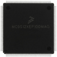
MC9S12XEP100MAG Freescale Semiconductor, MC9S12XEP100MAG Datasheet - Page 386

MC9S12XEP100MAG
Manufacturer Part Number
MC9S12XEP100MAG
Description
IC MCU 16BIT 1M FLASH 144-LQFP
Manufacturer
Freescale Semiconductor
Series
HCS12r
Datasheet
1.MC9S12XEP768CAL.pdf
(1328 pages)
Specifications of MC9S12XEP100MAG
Core Processor
HCS12X
Core Size
16-Bit
Speed
50MHz
Connectivity
CAN, EBI/EMI, I²C, IrDA, SCI, SPI
Peripherals
LVD, POR, PWM, WDT
Number Of I /o
119
Program Memory Size
1MB (1M x 8)
Program Memory Type
FLASH
Eeprom Size
4K x 8
Ram Size
64K x 8
Voltage - Supply (vcc/vdd)
1.72 V ~ 5.5 V
Data Converters
A/D 24x12b
Oscillator Type
External
Operating Temperature
-40°C ~ 125°C
Package / Case
144-LQFP
Processor Series
S12XE
Core
HCS12
Data Bus Width
16 bit
Data Ram Size
64 KB
Interface Type
CAN/SCI/SPI
Maximum Clock Frequency
50 MHz
Number Of Programmable I/os
119
Number Of Timers
25
Maximum Operating Temperature
+ 125 C
Mounting Style
SMD/SMT
3rd Party Development Tools
EWHCS12
Development Tools By Supplier
KIT33812ECUEVME, EVB9S12XEP100, DEMO9S12XEP100
Minimum Operating Temperature
- 40 C
On-chip Adc
24-ch x 12-bit
For Use With
EVB9S12XEP100 - BOARD EVAL FOR MC9S12XEP100DEMO9S12XEP100 - BOARD DEMO FOR MC9S12XEP100
Lead Free Status / RoHS Status
Lead free / RoHS Compliant
Available stocks
Company
Part Number
Manufacturer
Quantity
Price
Company:
Part Number:
MC9S12XEP100MAG
Manufacturer:
Freescale Semiconductor
Quantity:
135
Company:
Part Number:
MC9S12XEP100MAG
Manufacturer:
FREESCAL
Quantity:
255
Company:
Part Number:
MC9S12XEP100MAG
Manufacturer:
Freescale Semiconductor
Quantity:
10 000
Part Number:
MC9S12XEP100MAG
Manufacturer:
FREESCALE
Quantity:
20 000
- Current page: 386 of 1328
- Download datasheet (9Mb)
Chapter 10 XGATE (S12XGATEV3)
10.8.1.8
In this mode the result of an operation between two registers is stored in one of the registers used as
operands.
RD = RD ∗ RS is the general register to register format, with register RD being the first operand and RS
the second. RD and RS can be any of the 8 general purpose registers R0 … R7. If R0 is used as the
destination register, only the condition code flags are updated. This addressing mode is used only for shift
operations with a variable shift value
Examples:
10.8.1.9
In this mode the result of an operation between two or three registers is stored into a third one.
RD = RS1 ∗ RS2 is the general format used in the order RD, RS1, RS1. RD, RS1, RS2 can be any of the
8 general purpose registers R0 … R7. If R0 is used as the destination register RD, only the condition code
flags are updated. This addressing mode is used for all arithmetic and logical operations.
Examples:
10.8.1.10 Relative Addressing 9-Bit Wide (REL9)
A 9-bit signed word address offset is included in the instruction word. This addressing mode is used for
conditional branch instructions.
Examples:
10.8.1.11 Relative Addressing 10-Bit Wide (REL10)
An 10-bit signed word address offset is included in the instruction word. This addressing mode is used for
the unconditional branch instruction.
Examples:
10.8.1.12 Index Register plus Immediate Offset (IDO5)
(RS, #OFFS5) provides an unsigned offset from the base register.
Examples:
386
Because of an order from the United States International Trade Commission, BGA-packaged product lines and partnumbers
indicated here currently are not available from Freescale for import or sale in the United States prior to September 2010
LSL
LSR
ADC
SUB
BCC
BEQ
BRA
LDB
STW
Dyadic Addressing (DYA)
Triadic Addressing (TRI)
R4,R5
R4,R5
R5,R6,R7
R5,R6,R7
REL9
REL9
REL10
R4,(R1,#OFFS5)
R4,(R1,#OFFS5)
; R4 = R4 << R5
; R4 = R4 >> R5
MC9S12XE-Family Reference Manual , Rev. 1.23
; R5 = R6 + R7 + Carry
; R5 = R6 - R7
; PC = PC + 2 + (REL9 << 1)
; PC = PC + 2 + (REL9 << 1)
; PC = PC + 2 + (REL10 << 1)
; loads a byte from (R1+OFFS5) into R4
; stores R4 as a word to (R1+OFFS5)
Freescale Semiconductor
Related parts for MC9S12XEP100MAG
Image
Part Number
Description
Manufacturer
Datasheet
Request
R
Part Number:
Description:
Manufacturer:
Freescale Semiconductor, Inc
Datasheet:
Part Number:
Description:
Manufacturer:
Freescale Semiconductor, Inc
Datasheet:
Part Number:
Description:
Manufacturer:
Freescale Semiconductor, Inc
Datasheet:
Part Number:
Description:
Manufacturer:
Freescale Semiconductor, Inc
Datasheet:
Part Number:
Description:
Manufacturer:
Freescale Semiconductor, Inc
Datasheet:
Part Number:
Description:
Manufacturer:
Freescale Semiconductor, Inc
Datasheet:
Part Number:
Description:
Manufacturer:
Freescale Semiconductor, Inc
Datasheet:
Part Number:
Description:
Manufacturer:
Freescale Semiconductor, Inc
Datasheet:
Part Number:
Description:
Manufacturer:
Freescale Semiconductor, Inc
Datasheet:
Part Number:
Description:
Manufacturer:
Freescale Semiconductor, Inc
Datasheet:
Part Number:
Description:
Manufacturer:
Freescale Semiconductor, Inc
Datasheet:
Part Number:
Description:
Manufacturer:
Freescale Semiconductor, Inc
Datasheet:
Part Number:
Description:
Manufacturer:
Freescale Semiconductor, Inc
Datasheet:
Part Number:
Description:
Manufacturer:
Freescale Semiconductor, Inc
Datasheet:
Part Number:
Description:
Manufacturer:
Freescale Semiconductor, Inc
Datasheet:


