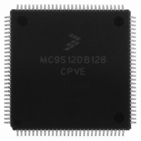
MC9S12DB128CPVE Freescale Semiconductor, MC9S12DB128CPVE Datasheet - Page 61

MC9S12DB128CPVE
Manufacturer Part Number
MC9S12DB128CPVE
Description
IC MCU 128K FLASH 25MHZ 112-LQFP
Manufacturer
Freescale Semiconductor
Series
HCS12r
Datasheets
1.MC9S12DG128CFUER.pdf
(128 pages)
2.MC9S12DB128CPVE.pdf
(142 pages)
3.MC9S12DB128CPVE.pdf
(12 pages)
Specifications of MC9S12DB128CPVE
Core Processor
HCS12
Core Size
16-Bit
Speed
25MHz
Connectivity
CAN, I²C, SCI, SPI
Peripherals
PWM, WDT
Number Of I /o
91
Program Memory Size
128KB (128K x 8)
Program Memory Type
FLASH
Eeprom Size
2K x 8
Ram Size
8K x 8
Voltage - Supply (vcc/vdd)
2.35 V ~ 5.25 V
Data Converters
A/D 16x10b
Oscillator Type
Internal
Operating Temperature
-40°C ~ 85°C
Package / Case
112-LQFP
Controller Family/series
HCS12/S12X
No. Of I/o's
91
Eeprom Memory Size
2048Byte
Ram Memory Size
8192Byte
Cpu Speed
25MHz
Rohs Compliant
Yes
Package
112LQFP
Family Name
HCS12
Maximum Speed
50 MHz
Operating Supply Voltage
3.3|5 V
Data Bus Width
16 Bit
Number Of Programmable I/os
91
Interface Type
CAN/SCI/SPI
On-chip Adc
2(8-chx10-bit)
Number Of Timers
8
Lead Free Status / RoHS Status
Lead free / RoHS Compliant
Available stocks
Company
Part Number
Manufacturer
Quantity
Price
Company:
Part Number:
MC9S12DB128CPVE
Manufacturer:
Freescale Semiconductor
Quantity:
10 000
Company:
Part Number:
MC9S12DB128CPVER
Manufacturer:
Freescale Semiconductor
Quantity:
10 000
Freescale Semiconductor, Inc.
MC9S12DT128B Device User Guide — V01.09
2.3.21 PH6 / KWH6 — Port H I/O Pin 6
PH6 is a general purpose input or output pin. It can be configured to generate an interrupt causing the MCU
to exit STOP or WAIT mode.
2.3.22 PH5 / KWH5 — Port H I/O Pin 5
PH5 is a general purpose input or output pin. It can be configured to generate an interrupt causing the MCU
to exit STOP or WAIT mode.
2.3.23 PH4 / KWH4 — Port H I/O Pin 2
PH4 is a general purpose input or output pin. It can be configured to generate an interrupt causing the MCU
to exit STOP or WAIT mode.
2.3.24 PH3 / KWH3 / SS1 — Port H I/O Pin 3
PH3 is a general purpose input or output pin. It can be configured to generate an interrupt causing the MCU
to exit STOP or WAIT mode. It can be configured as slave select pin SS of the Serial Peripheral Interface
1 (SPI1).
2.3.25 PH2 / KWH2 / SCK1 — Port H I/O Pin 2
PH2 is a general purpose input or output pin. It can be configured to generate an interrupt causing the MCU
to exit STOP or WAIT mode. It can be configured as serial clock pin SCK of the Serial Peripheral Interface
1 (SPI1).
2.3.26 PH1 / KWH1 / MOSI1 — Port H I/O Pin 1
PH1 is a general purpose input or output pin. It can be configured to generate an interrupt causing the MCU
to exit STOP or WAIT mode. It can be configured as master output (during master mode) or slave input
pin (during slave mode) MOSI of the Serial Peripheral Interface 1 (SPI1).
2.3.27 PH0 / KWH0 / MISO1 — Port H I/O Pin 0
PH0 is a general purpose input or output pin. It can be configured to generate an interrupt causing the MCU
to exit STOP or WAIT mode. It can be configured as master input (during master mode) or slave output
(during slave mode) pin MISO of the Serial Peripheral Interface 1 (SPI1).
2.3.28 PJ7 / KWJ7 / TXCAN4 / SCL — PORT J I/O Pin 7
PJ7 is a general purpose input or output pin. It can be configured to generate an interrupt causing the MCU
to exit STOP or WAIT mode. It can be configured as the transmit pin TXCAN for the Motorola Scalable
Controller Area Network controller 4 (CAN4) or the serial clock pin SCL of the IIC module.
For More Information On This Product,
Go to: www.freescale.com


