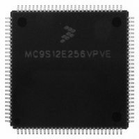
MC9S12E256VPVE Freescale Semiconductor, MC9S12E256VPVE Datasheet - Page 562

MC9S12E256VPVE
Manufacturer Part Number
MC9S12E256VPVE
Description
IC MCU 256K FLASH 25MHZ 112-LQFP
Manufacturer
Freescale Semiconductor
Series
HCS12r
Datasheet
1.MC9S12E256CFUE.pdf
(602 pages)
Specifications of MC9S12E256VPVE
Core Processor
HCS12
Core Size
16-Bit
Speed
25MHz
Connectivity
EBI/EMI, I²C, SCI, SPI
Peripherals
POR, PWM, WDT
Number Of I /o
91
Program Memory Size
256KB (256K x 8)
Program Memory Type
FLASH
Ram Size
16K x 8
Voltage - Supply (vcc/vdd)
2.35 V ~ 2.75 V
Data Converters
A/D 16x10b; D/A 2x8b
Oscillator Type
Internal
Operating Temperature
-40°C ~ 105°C
Package / Case
112-LQFP
Processor Series
S12E
Core
HCS12
Data Bus Width
16 bit
Data Ram Size
16 KB
Interface Type
I2C/SCI/SPI
Maximum Clock Frequency
50 MHz
Number Of Programmable I/os
92
Number Of Timers
12
Maximum Operating Temperature
+ 105 C
Mounting Style
SMD/SMT
3rd Party Development Tools
EWHCS12
Minimum Operating Temperature
- 40 C
On-chip Adc
16-ch x 10-bit
On-chip Dac
2-ch x 8-bit
For Use With
M68EVB912E128 - BOARD EVAL FOR MC9S12E128/64
Lead Free Status / RoHS Status
Lead free / RoHS Compliant
Eeprom Size
-
Lead Free Status / Rohs Status
Lead free / RoHS Compliant
Available stocks
Company
Part Number
Manufacturer
Quantity
Price
Company:
Part Number:
MC9S12E256VPVE
Manufacturer:
Freescale Semiconductor
Quantity:
10 000
- Current page: 562 of 602
- Download datasheet (4Mb)
Appendix A Electrical Characteristics
A.1.5
Absolute maximum ratings are stress ratings only. A functional operation under or outside those maxima
is not guaranteed. Stress beyond those limits may affect the reliability or cause permanent damage of the
device.
This device contains circuitry protecting against damage due to high static voltage or electrical fields;
however, it is advised that normal precautions be taken to avoid application of any voltages higher than
maximum-rated voltages to this high-impedance circuit. Reliability of operation is enhanced if unused
inputs are tied to an appropriate logic voltage level (e.g., either V
1
2
3
4
562
Num
The device contains an internal voltage regulator to generate the logic and PLL supply out of the I/O supply. The absolute
maximum ratings apply when the device is powered from an external source.
All digital I/O pins are internally clamped to V
These pins are internally clamped to V
This pin is clamped low to V
10
11
12
13
14
15
1
2
3
4
5
6
7
8
9
I/O, Regulator and Analog Supply Voltage
Internal Logic Supply Voltage
PLL Supply Voltage
Voltage difference VDDX to VDDR and VDDA
Voltage difference VSSX to VSSR and VSSA
Digital I/O Input Voltage
Analog Reference
XFC, EXTAL, XTAL inputs
TEST input
Instantaneous Maximum Current
Instantaneous Maximum Current
Instantaneous Maximum Current
Operating Temperature Range (packaged)
Operating Temperature Range (junction)
Storage Temperature Range
Single pin limit for all digital I/O pins
Single pin limit for XFC, EXTAL, XTAL
Single pin limit for TEST
Absolute Maximum Ratings
1
SSR
, but not clamped high. This pin must be tied low in applications.
4
Rating
1
Table A-1. Absolute Maximum Ratings
SSPLL
MC9S12E256 Data Sheet, Rev. 1.08
and V
SSX
2
3
and V
DDPLL
DDX
, V
SSR
and V
DDR
V
Symbol
V
SS5
or V
V
RH,
V
DDPLL
T stg
V
V
VDDX
VSSX
V
TEST
I
I
T
T
DD5
I
DL
DT
DD
ILV
D
IN
A
J
V
SSA
or V
RL
and V
DD5
DDA
–0.25
).
–0.3
–0.3
–0.3
–0.3
–0.3
–0.3
–0.3
–0.3
–0.3
– 40
– 40
– 65
Min
–25
–25
.
Freescale Semiconductor
Max
10.0
+25
+25
125
140
155
6.5
3.0
3.0
0.3
0.3
6.5
6.5
3.0
0
Unit
mA
mA
mA
V
V
V
V
V
V
V
V
V
C
C
C
Related parts for MC9S12E256VPVE
Image
Part Number
Description
Manufacturer
Datasheet
Request
R
Part Number:
Description:
Manufacturer:
Freescale Semiconductor, Inc
Datasheet:
Part Number:
Description:
Manufacturer:
Freescale Semiconductor, Inc
Datasheet:
Part Number:
Description:
Manufacturer:
Freescale Semiconductor, Inc
Datasheet:
Part Number:
Description:
Manufacturer:
Freescale Semiconductor, Inc
Datasheet:
Part Number:
Description:
Manufacturer:
Freescale Semiconductor, Inc
Datasheet:
Part Number:
Description:
Manufacturer:
Freescale Semiconductor, Inc
Datasheet:
Part Number:
Description:
Manufacturer:
Freescale Semiconductor, Inc
Datasheet:
Part Number:
Description:
Manufacturer:
Freescale Semiconductor, Inc
Datasheet:
Part Number:
Description:
Manufacturer:
Freescale Semiconductor, Inc
Datasheet:
Part Number:
Description:
Manufacturer:
Freescale Semiconductor, Inc
Datasheet:
Part Number:
Description:
Manufacturer:
Freescale Semiconductor, Inc
Datasheet:
Part Number:
Description:
Manufacturer:
Freescale Semiconductor, Inc
Datasheet:
Part Number:
Description:
Manufacturer:
Freescale Semiconductor, Inc
Datasheet:
Part Number:
Description:
Manufacturer:
Freescale Semiconductor, Inc
Datasheet:
Part Number:
Description:
Manufacturer:
Freescale Semiconductor, Inc
Datasheet:


