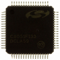
C8051F133-GQ Silicon Laboratories Inc, C8051F133-GQ Datasheet - Page 115

C8051F133-GQ
Manufacturer Part Number
C8051F133-GQ
Description
IC 8051 MCU 64K FLASH 64TQFP
Manufacturer
Silicon Laboratories Inc
Series
C8051F13xr
Specifications of C8051F133-GQ
Program Memory Type
FLASH
Program Memory Size
64KB (64K x 8)
Package / Case
64-TQFP, 64-VQFP
Core Processor
8051
Core Size
8-Bit
Speed
100MHz
Connectivity
EBI/EMI, SMBus (2-Wire/I²C), SPI, UART/USART
Peripherals
Brown-out Detect/Reset, POR, PWM, Temp Sensor, WDT
Number Of I /o
32
Ram Size
8.25K x 8
Voltage - Supply (vcc/vdd)
3 V ~ 3.6 V
Data Converters
A/D 8x10b
Oscillator Type
Internal
Operating Temperature
-40°C ~ 85°C
Processor Series
C8051F1x
Core
8051
Data Bus Width
8 bit
Data Ram Size
8.25 KB
Interface Type
I2C/SMBus/SPI/UART
Maximum Clock Frequency
100 MHz
Number Of Programmable I/os
32
Number Of Timers
5
Operating Supply Voltage
2.7 V to 3.6 V
Maximum Operating Temperature
+ 85 C
Mounting Style
SMD/SMT
3rd Party Development Tools
PK51, CA51, A51, ULINK2
Development Tools By Supplier
C8051F120DK
Minimum Operating Temperature
- 40 C
On-chip Adc
8-ch x 10-bit
No. Of I/o's
32
Ram Memory Size
8448Byte
Cpu Speed
100MHz
No. Of Timers
5
Rohs Compliant
Yes
Lead Free Status / RoHS Status
Lead free / RoHS Compliant
Eeprom Size
-
Lead Free Status / Rohs Status
Lead free / RoHS Compliant
Other names
336-1235
Available stocks
Company
Part Number
Manufacturer
Quantity
Price
Company:
Part Number:
C8051F133-GQ
Manufacturer:
SILICON
Quantity:
5
Company:
Part Number:
C8051F133-GQ
Manufacturer:
SiliconL
Quantity:
570
Company:
Part Number:
C8051F133-GQ
Manufacturer:
Silicon Laboratories Inc
Quantity:
10 000
Company:
Part Number:
C8051F133-GQR
Manufacturer:
ST
Quantity:
101
Company:
Part Number:
C8051F133-GQR
Manufacturer:
Silicon Laboratories Inc
Quantity:
10 000
- Current page: 115 of 350
- Download datasheet (2Mb)
9.2.
On the C8051F121/3/5/7 devices, the REF0CN register also allows selection of the voltage reference
source for ADC0 and ADC2, as shown in SFR Definition 9.2. Bits AD0VRS and AD2VRS in the REF0CN
register select the ADC0 and ADC2 voltage reference sources, respectively. The VREFA pin provides a
voltage reference input for ADC0 and ADC2, which can be connected to an external precision reference or
the internal voltage reference. ADC0 may also reference the DAC0 output internally, and ADC2 may refer-
ence the analog power supply voltage, via the VREF multiplexers shown in Figure 9.2.
Figure 9.2. Voltage Reference Functional Block Diagram (C8051F121/3/5/7)
Reference Configuration on the C8051F121/3/5/7
Reference
External
Voltage
Circuit
DGND
VDD
Recommended Bypass
4.7F
R1
Capacitors
+
0.1F
VREFA
VREF
Rev. 1.4
REF0CN
C8051F120/1/2/3/4/5/6/7
DAC0
DAC1
Ref
REFBE
x2
AV+
1
0
0
1
C8051F130/1/2/3
Band-Gap
BIASE
1.2V
EN
ADC2
ADC0
Ref
Ref
Bias to
ADCs,
DACs
115
Related parts for C8051F133-GQ
Image
Part Number
Description
Manufacturer
Datasheet
Request
R
Part Number:
Description:
SMD/C°/SINGLE-ENDED OUTPUT SILICON OSCILLATOR
Manufacturer:
Silicon Laboratories Inc
Part Number:
Description:
Manufacturer:
Silicon Laboratories Inc
Datasheet:
Part Number:
Description:
N/A N/A/SI4010 AES KEYFOB DEMO WITH LCD RX
Manufacturer:
Silicon Laboratories Inc
Datasheet:
Part Number:
Description:
N/A N/A/SI4010 SIMPLIFIED KEY FOB DEMO WITH LED RX
Manufacturer:
Silicon Laboratories Inc
Datasheet:
Part Number:
Description:
N/A/-40 TO 85 OC/EZLINK MODULE; F930/4432 HIGH BAND (REV E/B1)
Manufacturer:
Silicon Laboratories Inc
Part Number:
Description:
EZLink Module; F930/4432 Low Band (rev e/B1)
Manufacturer:
Silicon Laboratories Inc
Part Number:
Description:
I°/4460 10 DBM RADIO TEST CARD 434 MHZ
Manufacturer:
Silicon Laboratories Inc
Part Number:
Description:
I°/4461 14 DBM RADIO TEST CARD 868 MHZ
Manufacturer:
Silicon Laboratories Inc
Part Number:
Description:
I°/4463 20 DBM RFSWITCH RADIO TEST CARD 460 MHZ
Manufacturer:
Silicon Laboratories Inc
Part Number:
Description:
I°/4463 20 DBM RADIO TEST CARD 868 MHZ
Manufacturer:
Silicon Laboratories Inc
Part Number:
Description:
I°/4463 27 DBM RADIO TEST CARD 868 MHZ
Manufacturer:
Silicon Laboratories Inc
Part Number:
Description:
I°/4463 SKYWORKS 30 DBM RADIO TEST CARD 915 MHZ
Manufacturer:
Silicon Laboratories Inc
Part Number:
Description:
N/A N/A/-40 TO 85 OC/4463 RFMD 30 DBM RADIO TEST CARD 915 MHZ
Manufacturer:
Silicon Laboratories Inc
Part Number:
Description:
I°/4463 20 DBM RADIO TEST CARD 169 MHZ
Manufacturer:
Silicon Laboratories Inc


