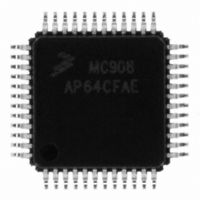
MC908AP64CFAE Freescale Semiconductor, MC908AP64CFAE Datasheet - Page 234

MC908AP64CFAE
Manufacturer Part Number
MC908AP64CFAE
Description
IC MCU 64K 8MHZ SPI 48-LQFP
Manufacturer
Freescale Semiconductor
Series
HC08r
Specifications of MC908AP64CFAE
Core Processor
HC08
Core Size
8-Bit
Speed
8MHz
Connectivity
I²C, IRSCI, SCI, SPI
Peripherals
LED, LVD, POR, PWM
Number Of I /o
32
Program Memory Size
64KB (64K x 8)
Program Memory Type
FLASH
Ram Size
2K x 8
Voltage - Supply (vcc/vdd)
2.7 V ~ 5.5 V
Data Converters
A/D 8x10b
Oscillator Type
Internal
Operating Temperature
-40°C ~ 85°C
Package / Case
48-LQFP
Cpu Family
HC08
Device Core Size
8b
Frequency (max)
8MHz
Interface Type
SCI/SPI
Total Internal Ram Size
2KB
# I/os (max)
32
Number Of Timers - General Purpose
4
Operating Supply Voltage (typ)
3.3/5V
Operating Supply Voltage (max)
5.5V
Operating Supply Voltage (min)
2.7V
On-chip Adc
8-chx10-bit
Instruction Set Architecture
CISC
Operating Temp Range
-40C to 85C
Operating Temperature Classification
Industrial
Mounting
Surface Mount
Pin Count
48
Package Type
LQFP
Controller Family/series
HC08
No. Of I/o's
32
Ram Memory Size
2KB
Cpu Speed
8MHz
No. Of Timers
2
Embedded Interface Type
I2C, SCI, SPI
Rohs Compliant
Yes
Processor Series
HC08AP
Core
HC08
Data Bus Width
8 bit
Data Ram Size
2 KB
Maximum Clock Frequency
8 MHz
Number Of Programmable I/os
32
Number Of Timers
4
Maximum Operating Temperature
+ 85 C
Mounting Style
SMD/SMT
Development Tools By Supplier
FSICEBASE, DEMO908AP64E, M68CBL05CE
Minimum Operating Temperature
- 40 C
Package
48LQFP
Family Name
HC08
Maximum Speed
8 MHz
Operating Supply Voltage
3.3|5 V
Lead Free Status / RoHS Status
Lead free / RoHS Compliant
Eeprom Size
-
Lead Free Status / Rohs Status
Compliant
Available stocks
Company
Part Number
Manufacturer
Quantity
Price
Company:
Part Number:
MC908AP64CFAE
Manufacturer:
Freescale
Quantity:
3 359
Company:
Part Number:
MC908AP64CFAE
Manufacturer:
Freescale Semiconductor
Quantity:
10 000
Company:
Part Number:
MC908AP64CFAER
Manufacturer:
Freescale Semiconductor
Quantity:
10 000
- Current page: 234 of 324
- Download datasheet (4Mb)
Multi-Master IIC Interface (MMIIC)
Only the slave with a matched address will respond by sending back an acknowledge bit by pulling SDA
low on the 9th clock cycle.
(See
Figure
14-2.)
14.5.3 Data Transfer
Once a successful slave addressing is achieved, the data transfer can proceed byte by byte in the
direction specified by the R/W-bit sent by the calling master.
Each data byte is 8 bits. Data can be changed only when SCL is low and must be held stable when SCL
is high as shown in
Figure
14-2. The MSB is transmitted first and each byte has to be followed by an
acknowledge bit. This is signalled by the receiving device by pulling the SDA low on the 9th clock cycle.
Therefore, one complete data byte transfer requires 9 clock cycles.
If the slave receiver does not acknowledge the master, the SDA line should be left high by the slave. The
master can then generate a STOP signal to abort the data transfer or a START signal (repeated START)
to commence a new transfer.
If the master receiver does not acknowledge the slave transmitter after a byte has been transmitted, it
means an “end of data” to the slave. The slave should release the SDA line for the master to generate a
STOP or START signal.
14.5.4 Repeated START Signal
As shown in
Figure
14-2, a repeated START signal is used to generate START signal without first
generating a STOP to terminate the communication. This is used by the master to communicate with
another slave or with the same slave in a different mode (transmit/receive mode) without releasing the
bus.
14.5.5 STOP Signal
The master can terminate the communication by generating a STOP signal to free the bus. However, the
master may generate a START signal followed by a calling command without first generating a STOP
signal. This is called repeat START. A STOP signal is defined as a low to high transition of SDA while
SCL is at logic high (see
Figure
14-2).
14.5.6 Arbitration Procedure
The interface circuit is a multi-master system which allows more than one master to be connected. If two
or more masters try to control the bus at the same time, a clock synchronization procedure determines
the bus clock. The clock low period is equal to the longest clock low period and the clock high period is
equal to the shortest one among the masters. A data arbitration procedure determines the priority. A
master will lose arbitration if it transmits a logic 1 while another transmits a logic 0. The losing master will
immediately switch over to slave receive mode and stops its data and clock outputs. The transition from
master to slave will not generate a STOP condition. Meanwhile a software bit will be set by hardware to
indicates loss of arbitration.
14.5.7 Clock Synchronization
Since wired-AND logic is performed on SCL line, a high to low transition on the SCL line will affect the
devices connected to the bus. The devices start counting their low period once a device’s clock has gone
low, it will hold the SCL line low until the clock high state is reached. However, the change of low to high
MC68HC908AP Family Data Sheet, Rev. 4
232
Freescale Semiconductor
Related parts for MC908AP64CFAE
Image
Part Number
Description
Manufacturer
Datasheet
Request
R
Part Number:
Description:
Manufacturer:
Freescale Semiconductor, Inc
Datasheet:
Part Number:
Description:
Manufacturer:
Freescale Semiconductor, Inc
Datasheet:
Part Number:
Description:
Manufacturer:
Freescale Semiconductor, Inc
Datasheet:
Part Number:
Description:
Manufacturer:
Freescale Semiconductor, Inc
Datasheet:
Part Number:
Description:
Manufacturer:
Freescale Semiconductor, Inc
Datasheet:
Part Number:
Description:
Manufacturer:
Freescale Semiconductor, Inc
Datasheet:
Part Number:
Description:
Manufacturer:
Freescale Semiconductor, Inc
Datasheet:
Part Number:
Description:
Manufacturer:
Freescale Semiconductor, Inc
Datasheet:
Part Number:
Description:
Manufacturer:
Freescale Semiconductor, Inc
Datasheet:
Part Number:
Description:
Manufacturer:
Freescale Semiconductor, Inc
Datasheet:
Part Number:
Description:
Manufacturer:
Freescale Semiconductor, Inc
Datasheet:
Part Number:
Description:
Manufacturer:
Freescale Semiconductor, Inc
Datasheet:
Part Number:
Description:
Manufacturer:
Freescale Semiconductor, Inc
Datasheet:
Part Number:
Description:
Manufacturer:
Freescale Semiconductor, Inc
Datasheet:
Part Number:
Description:
Manufacturer:
Freescale Semiconductor, Inc
Datasheet:


